Introduce
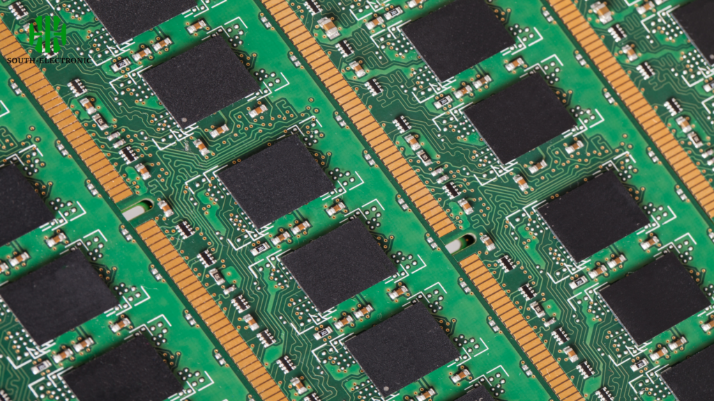
PCB panelization is a pivotal facet within the intricate realm of PCB manufacturing. This practice involves consolidating multiple PCBs onto a singular substrate, optimizing the utilization of production resources.
Importance
The significance of PCB panelization lies in its capacity to streamline production operations. By grouping multiple PCBs onto a single panel, manufacturers can capitalize on the substantial economies of scale afforded by bulk processing. This consolidation not only reduces manufacturing costs but also augments throughput, expediting the overall fabrication timeline.
PCB panelization addresses the spatial considerations inherent in manufacturing environments. It offers a judicious solution to the constraints posed by fabrication equipment, enabling the simultaneous processing of multiple boards. This practice is particularly pertinent in instances where the physical dimensions of the individual PCBs render standalone processing impractical.
PCB panelization transcends mere logistical expediency, it embodies a sophisticated orchestration of manufacturing processes aimed at maximizing economies of scale, minimizing operational bottlenecks, and ultimately optimizing the overarching efficiency of the PCB fabrication ecosystem.

Types of PCB panelization techniques
V-Score, a venerable technique in the realm of PCB manufacturing, entails the methodical scoring of the board's surface to facilitate precise and controlled breaking points. This method, akin to a surgical incision, allows for the seamless segmentation of multiple PCBs within a panel. The finesse of V-Score lies in its ability to achieve uniformity in separation, a critical attribute that not only expedites the manufacturing process but also minimizes the propensity for post-separation irregularities.
Tab Routing, a methodical symphony of precision and resilience, deploys strategically positioned tabs to interconnect individual PCBs within a panel. This technique is particularly germane in scenarios where intricate board geometries demand a meticulous approach or when fragility concerns necessitate structural fortification. The judicious utilization of tabs not only ensures structural integrity during the manufacturing process but also mitigates the risk of subsequent breakage, obviating the need for intricate post-processing interventions.
Grid Array Panelization, a paradigm of structural orchestration, involves the meticulous arrangement of PCBs within a matrix or grid formation on a singular panel. This method leverages a systematic grid layout to accommodate multiple boards, optimizing spatial efficiency and resource utilization. The symmetrical disposition within the grid array engenders a harmonious coexistence, fostering an environment where each PCB benefits from the economies of scale inherent in collective processing.
In essence, the selection among V-Score, Tab Routing, and Grid Array Panelization hinges on a careful consideration of design specifications, production priorities, and the desired balance between precision and structural robustness. V-Score ideal for rapid segmentation precision, Tab Routing for structural fortification, and Grid Array Panelization for spatial optimization. Each technique brings its unique strengths to the table, contributing to the overarching efficiency and effectiveness of the PCB manufacturing process.

Common challenges with PCB panelization
- Complex PCB designs with complex geometries pose significant challenges to seamless panelization.
- Different material properties and thicknesses on PCBs may hinder panelization uniformity.
- Integration of panelized PCBs can create challenges during assembly and testing stages.
- Implement careful planning and leverage software tools that simulate assembly and test scenarios to identify and resolve potential bottlenecks upfront.
Optimization solutions and best practices
- Advanced Software Tools: Harness the power of cutting-edge software tools tailored specifically for PCB panelization. Tools such as AutoCAD, Altium Designer or Siemens NX not only facilitate precise panelization but also provide virtual simulation capabilities to help predict and solve potential challenges.
- Material Selection Guide: Establish comprehensive material selection guidelines to comply with the delicate requirements of panelization. Factors such as thermal conductivity, flexibility and mechanical strength are taken into account to ensure a harmonious combination of different materials within the panel.
- Collaboration between design and manufacturing teams: Facilitate seamless collaboration between design and manufacturing teams, bridging gaps to ensure panelization considerations are an integral part of the initial design phase. Establishing a symbiotic relationship between these key aspects of the production process enhances adaptability and facilitates simplified panelization.
Conclusion
In the labyrinth of PCB manufacturing, the art of panelization emerges as a strategic linchpin, orchestrating a harmonious dance between design intricacies and production efficiency. From the venerable precision of V-Score to the methodical symphony of Tab Routing and the structural orchestration in Grid Array Panelization, each technique plays a pivotal role in optimizing the overarching efficiency of the manufacturing ecosystem. Challenges inherent in complex designs and material variations find solutions through advanced software tools and meticulous material selection. The collaborative synergy between design and manufacturing teams becomes the catalyst for seamless panelization integration. As the industry continues to evolve, the judicious selection of panelization techniques stands as a testament to innovation, efficiency, and the continual pursuit of excellence.
