
In the DCDC power supply circuit, the layout of the PCB is very important for the realization of the circuit function and good various indicators. This article takes the buck circuit as an example to briefly analyze how to make a reasonable PCB layout and the precautions in the design.
Taking the simplest BUCK circuit topology as an example, the following figure indicates the direction of the current when the upper tube is turned on and off, that is, the power loop part. This part of the circuit is responsible for supplying power to the user load and bears a large power.
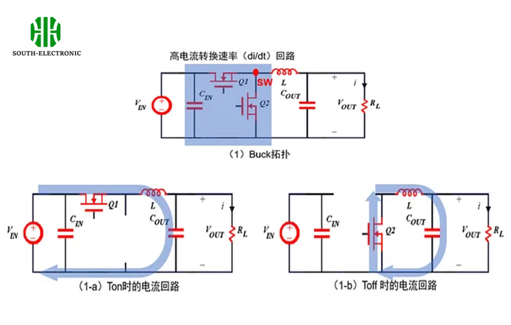
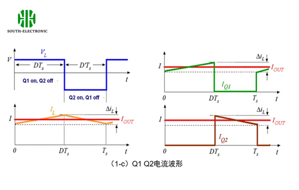
Combined with the current waveforms of Q1 and Q2 in the figure below, it is not difficult to find that due to the presence of inductance, there will be no higher current change trend in the second half of the circuit, and only in the part of the two switch tubes will there be a high current conversion rate. Special attention should be paid to PCB wiring to minimize the area of this fast-changing link as much as possible to reduce interference with other parts. With the advancement of integration technology, most power chips currently integrate the upper and lower tubes into the chip.
The power loop also needs to occupy as small a loop area as possible to reduce noise emission and parasitic parameters on the loop. The recommended PCB layout is shown in the figure above. Points to note are as follows:
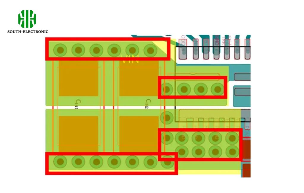
① The input capacitor is placed near the chip input Vin and power ground PGND to reduce the presence of parasitic inductance. Because the input current is discontinuous, the noise caused by parasitic inductance has an adverse effect on the chip’s withstand voltage and logic unit.
There is at least one decoupling capacitor next to the VIN pin to filter out the AC noise from the power input and the power noise from the inside of the chip (backflow), and also to store energy for the chip. The capacitor needs to be close to the pin, and the spacing between the two needs to be less than 40mil.
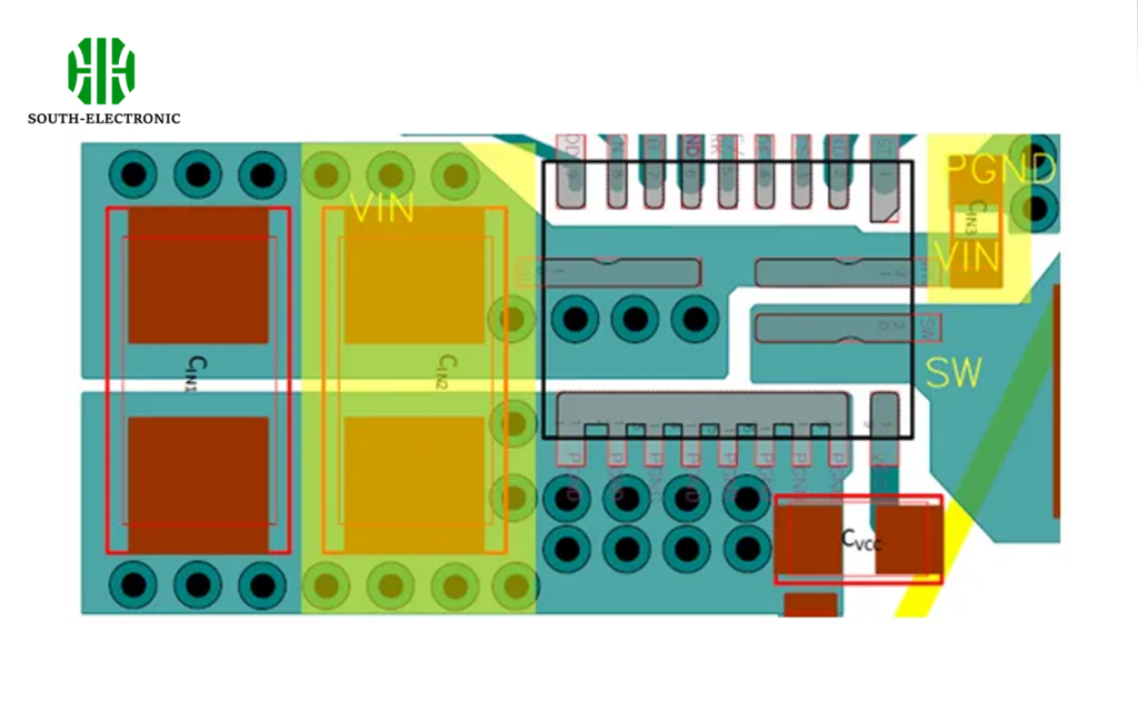
② The power loop should be as short and thick as possible, keeping the loop area small to reduce noise emission.
③ The SW point is a noise source. While ensuring the current, keep the area as small as possible and stay away from sensitive and susceptible locations.
④ The copper area and the number of vias will affect the PCB’s current carrying capacity and heat dissipation. Since the PCB’s current carrying capacity is related to the PCB board material, board thickness, wire width and thickness, and temperature rise, it is relatively complicated and can be accurately found and calculated through the IPC-2152 standard.
Generally speaking, more vias are needed at VIN (at least 6 vias) and PGND (at least 9 vias), and the copper at these two locations should be maximized to reduce parasitic impedance. The copper at SW also needs to be widened to avoid current limiting and abnormal operation.
For related designs, please refer to the following simple table:
| Design Recommendations | Weight (%) | Score | Self-Assessment | Notes |
|---|---|---|---|---|
| Component placement: Keep 40mil spacing. Place on the same layer as the chip. Input capacitors should be placed close to the chip. Decoupling capacitors need to be placed 6mil (minimum component spacing allowed) next to the VIN and power PGND pins, preferably not exceeding 20mil. | 15 | For power modules, this item can be ignored. | ||
| Inductor placement for power module: Place close to the SW pin. Put on the same layer as the chip. | 15 | For power modules, this item can be ignored. | ||
| Output capacitor placement: Both ends should be placed close to the Vout terminal of the inductor and power PGND. Put on the same layer as the chip. | 15 | |||
| Freewheeling diode placement: Need to be placed close to the inductor’s SW and power PGND. Put on the same layer as the chip. | 5 | For chips using synchronous power, this item can be ignored. | ||
| VCC capacitor placement: Should be placed close to the chip’s VCC pin. Put on the same layer as the chip. | 3 | |||
| FB resistor placement: Need to be placed close to the FB pin, with traces as short as possible. Put on the same layer as the chip. Keep away from noise sources. | 3 | |||
| BST RC placement: Need to be placed close to the SW and BST pins. Put on the same layer as the chip. | 3 | |||
| COMP RC placement: Place close to the corresponding pin. | 3 | If there is no such pin, this item can be ignored. | ||
| High-power network copper pouring – VIN copper pouring | 3 | |||
| High-power network copper pouring – SW copper pouring: The shorter the better under the condition of sufficient current-carrying capacity. | 4 | |||
| High-power network copper pouring – Vout copper pouring | 3 | |||
| High-power network copper pouring – GND copper pouring | 4 | It is more convenient to perform overall copper pouring at the end. | ||
| VIA holes – Quantity of GND network vias: (lin + lout)/200mA | 4 | |||
| VIA holes – Quantity of VIN network vias: lin/200mA | 3 | |||
| VIA holes – Quantity of Vout network vias: lin/200mA | 3 | |||
| VIA holes – Do not place vias on chip pins or component pads. | 1 | |||
| Other low-power signals – EN resistor: Try to place as close to the chip as possible; can be placed on different layers. | 1 | |||
| Other low-power signals – SS RC: Try to place as close to the chip pins as possible. | 1 | |||
| Other low-power signals – PG | 1 | |||
| Other low-power signals – Others (CS, mode, etc.) | 1 | Refer to the corresponding specification sheet. | ||
| Traces – Both traces and copper pours should use 45° or rounded corners. | 2 | |||
| Traces – No traces under the inductor. | 1 | |||
| Traces – Sampling signals: Route in parallel. | 1 | If there is no such function, this item can be ignored. |

