

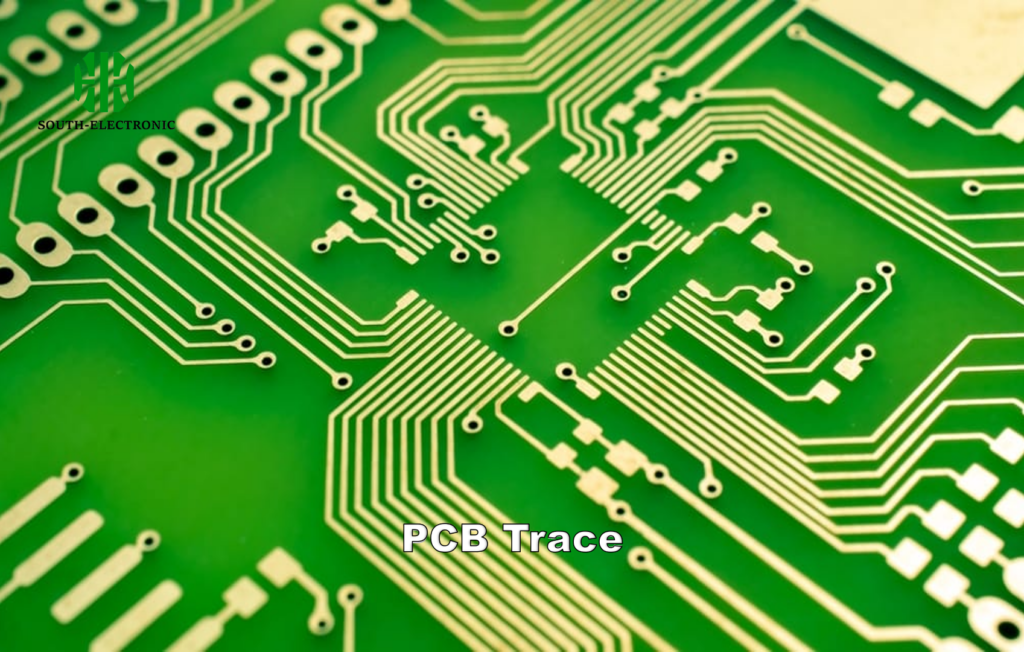
Did you inherit a legacy circuit board with no documentation? I once spent weeks staring at a mysterious PCB – until reverse engineering unlocked its secrets. Here’s how to systematically decode any board.
PCB reverse engineering[^1] methodically analyzes physical boards to recreate schematics and layouts. It helps restore undocumented designs, troubleshoot legacy systems[^2], or study competitor products, using disassembly, imaging software, and electrical validation to reconstruct circuit functionality.
Understanding PCB reverse engineering helps engineers resurrect obsolete systems and innovate faster. Let’s break down the practical process I’ve refined through trial and error.
What Is PCB Reverse Engineering and Why Use It?
When a critical medical device PCB failed, the manufacturer had vanished. Reverse engineering became our lifeline – but first, we needed strategic justification.
PCB reverse engineering extracts design knowledge from physical boards by documenting component placements[^3], tracing connections, and rebuilding schematics. Engineers use it to maintain obsolete systems, analyze competitor layouts, or recover lost designs – but must comply with IP laws.
)
Key Applications and Legal Considerations
While technically fascinating, reverse engineering carries legal risks. Here’s how to balance technical needs with compliance:
| Application | Technical Process | Legal Consideration |
|---|---|---|
| Legacy Maintenance | Document obsolete components | Check original licensing terms |
| Competitor Analysis | Compare circuit optimization | Avoid patent/copyright infringement |
| Design Recovery | Rebuild stolen/damaged board data | Prove original ownership |
| Educational Use | Study layout techniques | Follow fair use guidelines |
I always consult legal counsel before reverse engineering third-party boards. For internal legacy boards, maintain chain-of-custody documentation.
Using Reverse Engineering Software: How to Convert Images to Circuit Schematics
When my team scanned a 12-layer server board manually, errors piled up. Software tools transformed our workflow – but choosing the right one matters.
Specialized PCB reverse engineering software[^4] (like Altium, KiCad, or OpenRE) automates trace recognition from board scans. These tools convert layered images into editable schematics through pattern recognition, netlist generation, and 3D modeling – cutting manual work by 70%.
)
Software Comparison and Workflow
| Step | Manual Method | Software-Assisted | Time Savings |
|---|---|---|---|
| Component ID | Datasheet cross-referencing | Automated BOM generation | 65% |
| Trace Mapping | Multimeter probing | Image layer alignment algorithms | 80% |
| Schematic Creation | Hand-drawn diagrams | Auto-routing with error checking | 90% |
| Simulation | Physical prototyping | SPICE integration | 75% |
Modern tools can process high-resolution board scans into multilayer schematics in hours instead of weeks. However, manual verification remains crucial – I always cross-check 30% of automated connections.
How to Disassemble and Analyze the PCB Layout
A "simple" 4-layer audio board taught me harsh lessons about proper disassembly. Melted traces and lost components forced a restart.
Methodical PCB disassembly involves layer separation, chemical etching, and microscopic analysis. Use thermal profilers for safe layer removal, CNC mills for precision material removal, and SEM imaging for nanometer-scale trace inspection – preserving critical pads and vias.
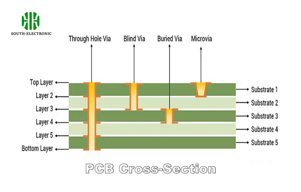)
Layer Analysis Techniques
| Layer Type | Analysis Tools | Key Parameters |
|---|---|---|
| Solder Mask | 3D surface profiler | Thickness uniformity ±5% |
| Copper Traces | Four-point probe tester | Conductivity ≥58 MS/m |
| Dielectric | TDR (Time Domain Reflectometry) | Impedance 50Ω ±10% |
| Plated Through-Hole | Cross-section microscopy | Plating thickness ≥25.4µm |
For multilayer boards, I sequentially document each layer’s components and interconnects. Annotated photos and impedance measurements help reconstruct the original design intent.
Is Your Reverse-Engineered PCB Ready for Production?
Our first reverse-engineered industrial controller failed spectacularly during EMI testing. Missing ground planes taught us rigorous validation steps.
Validate reverse-engineered PCBs with signal integrity simulations[^5] (HyperLynx), thermal analysis[^6] (ANSYS), and prototype testing. Check for compliance with IPC-2221 standards and original board’s environmental specs before mass production.
)
Production Validation Checklist
| Test Type | Pass Criteria | Tools/Methods |
|---|---|---|
| Electrical | ±5% voltage tolerance | Oscilloscope pattern matching |
| Thermal | <10°C hotspot variance | IR thermal imaging |
| Signal Integrity | Eye diagram mask compliance | Vector network analyzer |
| Environmental | 96hrs salt spray test passed | Climate chambers |
| Compliance | FCC/CE certifications | EMC test chambers |
I now run at least three prototype iterations – each addressing different failure modes from the previous version.
Conclusion
PCB reverse engineering combines meticulous disassembly, advanced software tools, and rigorous validation. Master these steps to resurrect legacy systems or derive technical insights safely and legally.
[^1]: Explore this link to gain a deeper understanding of PCB reverse engineering techniques and their applications in various industries.
[^2]: This resource will provide insights on maintaining and updating legacy systems, ensuring they remain functional and relevant.
[^3]: Learn about best practices for documenting component placements, which is crucial for effective PCB reverse engineering.
[^4]: Explore this link to discover top-rated PCB reverse engineering software that can enhance your workflow and accuracy.
[^5]: Discover how signal integrity simulations can enhance your PCB designs and prevent costly errors in production.
[^6]: Understanding thermal analysis is crucial for ensuring your PCB operates efficiently and reliably under various conditions.

