
New PCB designs often hide invisible killers – improper component spacing causes short circuits, arc flashes, and board fractures. These preventable failures cost engineers countless troubleshooting hours and companies expensive recalls. Proper safety spacing prevents these disasters before prototypes get manufactured.
PCB safety spacing[^1] protects circuits by maintaining critical distances between conductive elements. Designers must follow 0.2mm pad-to-pad spacing[^2] and 0.30mm copper-to-edge clearance rules while accounting for manufacturing tolerances, material expansion, and electrical stress factors.
While these numbers seem straightforward, real-world implementation requires understanding six key factors that dominate spacing decisions. Let’s examine the hidden variables that separate robust designs from potential disasters.
Why Is Proper Safety Spacing Critical in PCB Design?
A smartphone manufacturer once recalled 50,000 units when board-edge components cracked during assembly – all from ignoring 0.5mm clearance rules. This $2M mistake proves spacing isn’t just theoretical.
Adequate spacing prevents electrical arcing, mechanical stress damage, and manufacturing defects while ensuring compliance with international safety standards like IPC-2221[^3] and UL 60950-1.
)
Three Fundamental Spacing Requirements
| Spacing Type | Minimum Distance | Critical Factor |
|---|---|---|
| Conductor-to-edge | 0.40mm | Board routing & depaneling |
| High-voltage traces | 2.00mm per kV | Dielectric breakdown voltage |
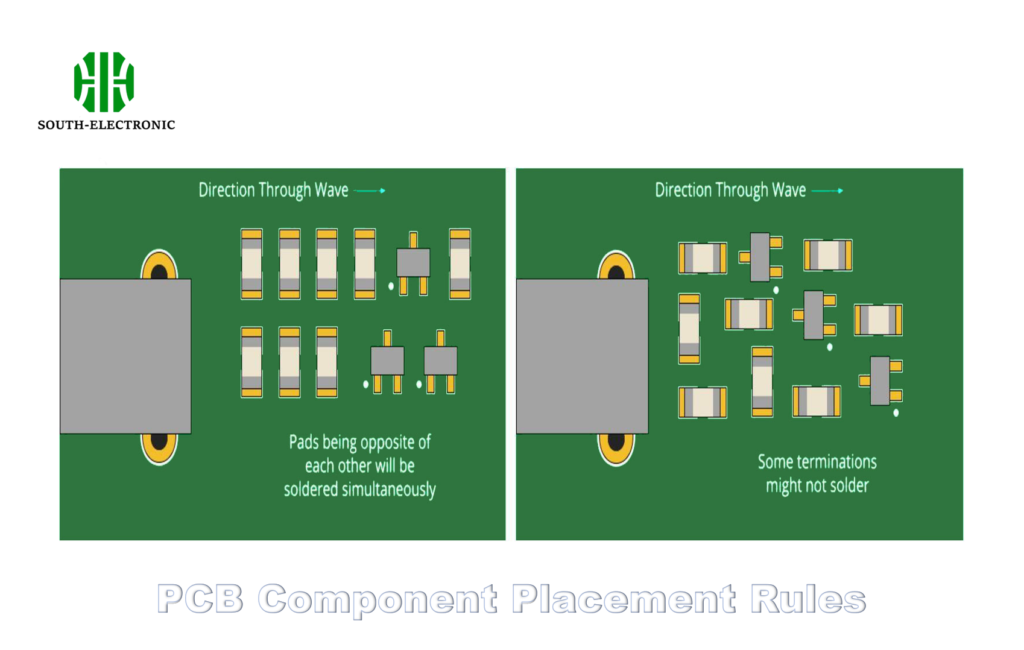
| SMD component bodies | 0.25mm | Wave soldering capillary flow |
Creepage distances increase exponentially with altitude – a 5,000m application needs 150% more spacing than sea-level designs. Always cross-reference your operating environment against IEC 60664-1 altitude derating tables.
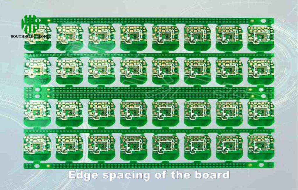
What Key Factors Determine Component-to-Edge Clearance?
An automotive control module failed EMI tests because chips placed 0.28mm from the edge created antenna effects. The fix? Increasing clearance to 0.35mm solved the interference.
Edge clearance depends on board thickness, depaneling method (V-cut vs routing), and component height[^4]. Thinner 0.8mm boards require 25% more clearance than standard 1.6mm substrates.
)
Component Placement Matrix
| Factor | Impact on Clearance | Adjustment Method |
|---|---|---|
| Panelization | Increases needed | Add 0.15mm for V-cut channels |
| Conformal Coating | Reduces needed | Subtract 0.10mm with coating |
| Vibration Exposure | Increases needed | Add 0.20mm for automotive use |
| Copper Weight | Affects edge burrs | +0.05mm per oz over 1oz |
Always verify with your PCB vendor – some manufacturers require 0.50mm clearance for castellated holes versus 0.30mm for standard components. Castellations create irregular edges that need extra margin.
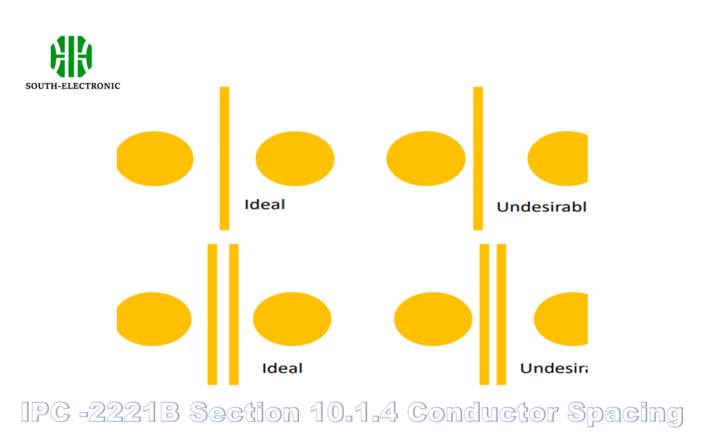
How Do IPC Standards Define Minimum Trace-to-Pad Spacing?
A medical device failed certification when 0.15mm trace-pad spacing[^5] allowed leakage currents. Bumping to 0.20mm brought it into IPC-2221A Class 2 compliance.
IPC-2221 specifies three spacing classes: 0.10mm (Class 1 consumer), 0.15mm (Class 2 industrial), and 0.20mm (Class 3 military/aerospace). These apply to inner layers – outer layers need 25% more clearance.
)
Voltage-Based Spacing Requirements
| Voltage (V) | Class 1 (mm) | Class 2 (mm) | Class 3 (mm) |
|---|---|---|---|
| ≤15 | 0.10 | 0.15 | 0.20 |
| 30 | 0.20 | 0.25 | 0.30 |
| 50 | 0.30 | 0.35 | 0.40 |
| 100 | 0.60 | 0.65 | 0.70 |
Remember – these are absolute minimums. Smart designers add 20% margin, creating 0.18mm spacing for Class 2 designs. This accommodates manufacturing tolerances and material warpage.
How to Validate Safety Spacing Using DFM Check Tools?
A designer found 23 spacing violations[^6] in their 4-layer board using real-time DFM checks – issues missed during manual review. These automated checks prevented $15k in scrapped prototypes.
Modern DFM tools[^7] like Altium’s Online DRC and Siemens’ Valor NPI automatically check against 200+ spacing rules. They simulate manufacturing outcomes including solder mask registration and etch compensation effects.
)
DFM Check Priority List
- Electrical clearance (traces/pads/vias)
- Copper-to-edge (board outline)
- Mask-to-copper (solder mask slivers)
- Legend-to-pad (silkscreen interference)
- Drill-to-copper (mechanical layer conflicts)
Run spacing checks at three stages: post-layout (full analysis), post-route (quick check), and pre-release (final verification). Always cross-validate with your PCB vendor’s capabilities document.
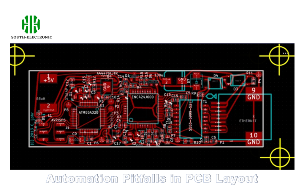
Can Automated Layout Tools Compromise Safety Spacing?
A router placed a via 0.18mm from the board edge to optimize trace length – violating the 0.30mm clearance rule. The "optimal" layout became unusable.
Auto-routers prioritize trace length over safety margins. Critical spacing requires manual constraints: set pad/via keepouts 0.35mm from edges and enable real-time DRC[^8] with 0.05mm tolerance buffers.
)
Router Setting Adjustments
| Parameter | Default Value | Safe Value |
|---|---|---|
| Edge clearance | 0.20mm | 0.35mm |
| Spacing priority | Speed | Reliability |
| Obstacle expansion | 0.00mm | 0.05mm |
| High-voltage net tag | Not applied | ≥50V nets |
Create separate design rules for critical areas like board edges and high-voltage sections. Use net classes to override general settings – a 100V power net needs different spacing than 3.3V logic signals.
Conclusion
PCB safety spacing combines precise measurements with practical application knowledge. By understanding IPC standards, material behaviors, and DFM validation tools, designers create reliable boards that survive real-world operation while passing stringent certifications.
[^1]: Understanding PCB safety spacing is crucial for preventing costly failures and ensuring compliance with safety standards. Explore this link to learn more.
[^2]: Discover the significance of 0.2mm pad-to-pad spacing in PCB design to avoid short circuits and enhance reliability.
[^3]: IPC-2221 outlines essential standards for PCB design. Understanding it can help you create safer and more reliable circuits.
[^4]: Understanding how component height affects clearance can help optimize your PCB layout for better performance and compliance.
[^5]: Learning about trace-pad spacing is crucial for preventing issues like leakage currents and ensuring your designs meet industry standards.
[^6]: Understanding common spacing violations can help you avoid costly mistakes in your PCB designs and improve quality.
[^7]: Explore this link to discover top DFM tools that can enhance your PCB design process and ensure safety spacing compliance.
[^8]: Learn how real-time DRC can prevent costly errors in PCB design and improve overall safety and reliability.

