Introduce
Among the various layers and components that constitute a PCB, the silkscreen layer stands out for its crucial role in communication rather than electrical function. This layer, often taken for granted, carries the vital signs and symbols that guide technicians, engineers, and assemblers through the complex geography of the board. This guide delves deep into the intricacies of PCB silkscreen printing, shedding light on its critical role, exploring varied methodologies, and highlighting the potential for customization.
What Is Silkscreen on a PCB?
Silkscreen on a PCB is essentially the text and symbols printed on the surface of the board. These markings can include component identifiers, test points, polarity symbols, and logos, along with warning or certification marks. Traditionally, the term “silkscreen” comes from the screen printing process once used to apply the ink, where a stencil made of silk was used to transfer the design.
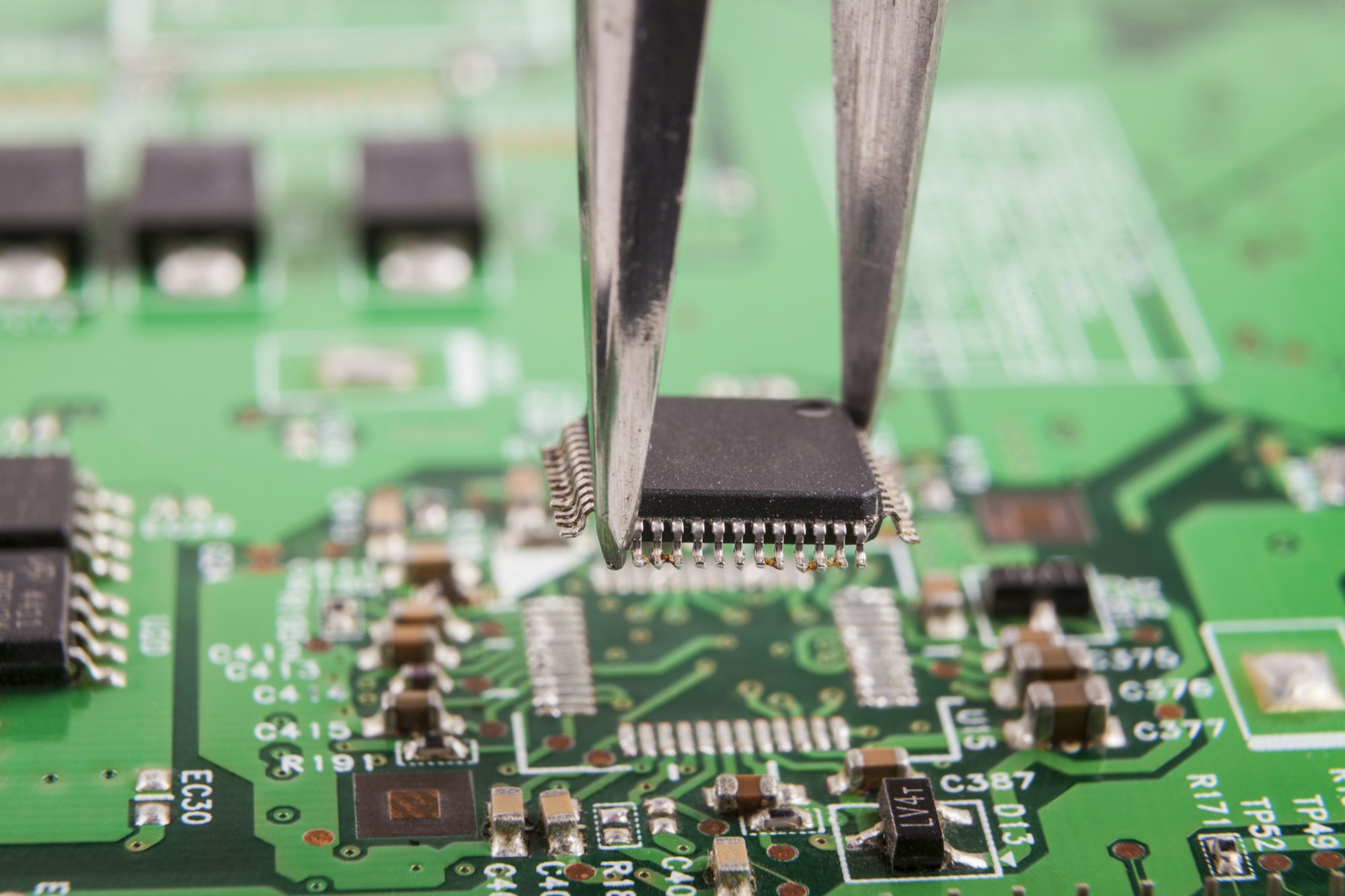
Silkscreen labels each component’s location on the PCB, identifying resistors, capacitors, integrated circuits, and other elements by unique reference designators. Without silkscreen, the risk of errors in component placement would dramatically increase, potentially leading to faulty products and increased waste.

3 Methods of Silkscreen Printing
Manual Screen Printing
Manual Screen Printing is the traditional approach to applying silkscreen on PCBs. This method involves creating a stencil or mesh screen that has been treated with a blocking stencil to impede the flow of ink through certain areas. Ink is then applied to the screen, and a squeegee is manually moved across the screen to press the ink through the open mesh and onto the PCB surface.
Advantages:
Cost-effectiveness for small to medium production runs.
Versatility in ink types and substrates.
Limitations:
Lower precision, making it less suitable for text and images requiring high detail.
Time-consuming setup, especially for multiple colors or complex designs.
Liquid Photo Imaging (LPI)
Liquid Photo Imaging represents a more modern technique that enhances the precision and uniformity of silkscreen markings. In this process, a photosensitive epoxy ink is applied to the entire surface of the PCB. The board is then exposed to ultraviolet (UV) light through a photomask that bears the desired markings, hardening the ink where exposed. Unexposed areas are then developed away, leaving a high-resolution image of the silkscreen.
Advantages:
High resolution and precision, suitable for fine texts and detailed graphics.
Good thickness control and durability of the markings.
Limitations:
More complex and costly setup compared to manual screen printing.
Requires a controlled environment to manage the photosensitive materials.
Direct Legend Printing (DLP)
Direct Legend Printing is a sophisticated method that employs digital printing techniques to apply the silkscreen directly onto the PCB without the need for physical stencils. DLP uses an inkjet or similar printer that deposits acrylic ink in accordance with the PCB’s design files.
dvantages:
High precision and adaptability to complex or frequently changing designs.
Eliminates the need for physical screens or masks, reducing setup times and costs.
Limitations:
The equipment costs and maintenance can be higher compared to traditional methods.
May not be as cost-effective for large volume production due to slower printing speeds.

Can silkscreen ink colors be customized?
Yes, silkscreen ink colors on Printed Circuit Boards (PCBs) can indeed be customized, offering manufacturers and designers flexibility in their PCB design and branding strategies. While the most commonly used silkscreen color is white, due to its excellent contrast against the typical green solder mask of PCBs, the industry is not limited to this standard. The customization of silkscreen ink colors on PCBs is not only feasible but also encouraged within the bounds of practical and regulatory considerations. This flexibility allows for enhanced aesthetic appeal, improved functionality, and adherence to brand identity, offering an additional layer of customization in PCB and electronic product design.

