Importance of Power Integrity (PI) and Power Distribution Networks (PDN)
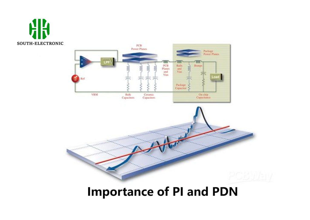
Power integrity is all about making sure your PCB can deliver clean, stable power to all the components on the board. If the power supply is noisy or fluctuating, your circuits won’t work right, your signals will degrade, and your device might not even work at all.
PDN is the system in a PCB that gets power from the supply to the parts. You want to make the PDN so that it has low impedance and noise, so that it can deliver power really well. In high-speed and high-density PCBs, where signal integrity and EMI are critical, PI and PDN are even more important.
Understanding Power Integrity (PI)
1.Definition and Key Concepts
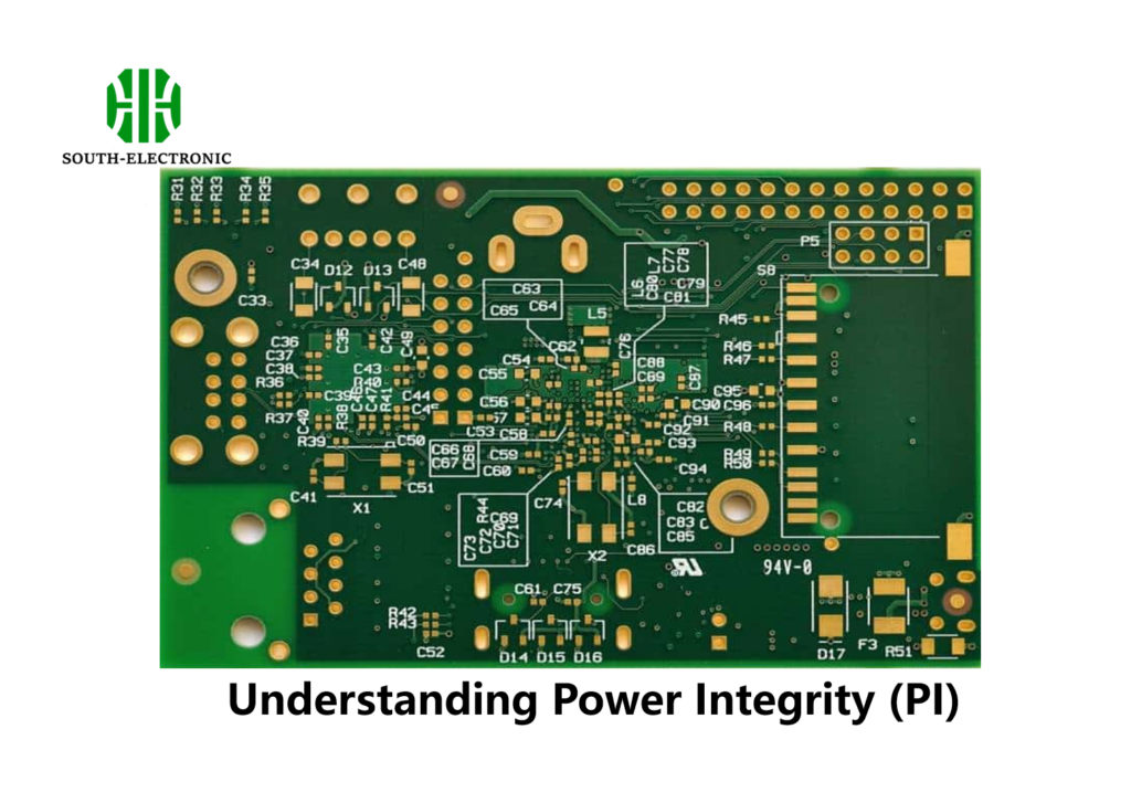
PI in PCBs is all about keeping a steady voltage at the power pins of every component on the board. Even tiny changes in voltage can cause digital circuits to make mistakes, which can mess up how well the whole thing works.
In high-speed PCBs, where signals change fast, any noise or change in the power supply can cause big problems. For example, voltage drops or noise on the power supply can make clock signals jitter or make logic gates switch wrong.
2.Challenges in PI for High-Speed and High-Density PCBs
Several challenges arise when trying to maintain power integrity in high-speed and high-density PCBs:
- Signal Integrity Issues: High-speed signals are more susceptible to noise, and any power fluctuation can introduce timing errors.
- Electromagnetic Interference (EMI): Dense component layouts can increase EMI, affecting both signal and power integrity.
- Voltage Fluctuations: High-density designs with multiple power planes can lead to uneven power distribution, causing voltage drops.
3.Methods to Improve PI
Improving power integrity in PCBs requires careful design and planning. Key methods include:
- Use of Decoupling Capacitors: Placing decoupling capacitors close to power pins helps filter out noise and stabilize voltage levels.
- PCB Layout Techniques: Minimize loop areas and ensure proper grounding to reduce noise and EMI.
- Power Plane Design: Use multiple power planes to distribute power evenly and reduce impedance.
Power Distribution Networks (PDN) in PCBs
1.What is a PDN?
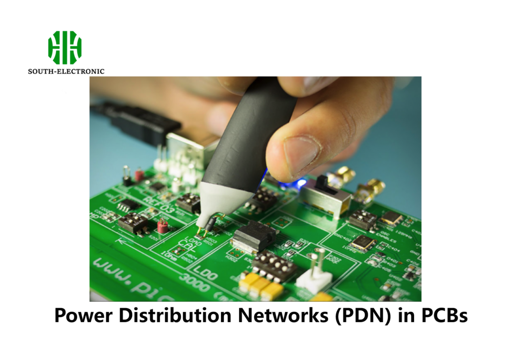
The Power Distribution Network (PDN) in a PCB is responsible for getting clean, stable power from the power supply to every component on the board. The PDN includes power planes, traces, vias, and decoupling capacitors, all working together to make sure each component gets the voltage it needs without noise or fluctuation.
2.Components of a PDN
A well-designed PDN consists of several key components:
- Power Planes: Large copper areas in the PCB that distribute power. They must be designed to minimize impedance and support high current loads.
- Vias: Conductive pathways that connect power planes across different layers of the PCB.
- Decoupling Capacitors: Positioned near components to filter out high-frequency noise and stabilize power.
3.PDN Design Considerations for High-Speed PCBs
Designing an effective PDN in high-speed PCBs requires attention to impedance, inductance, and capacitance:
- Low Impedance Paths: Ensuring low impedance in the PDN is critical to minimize voltage drops and noise.
- Proper Decoupling Strategies: Adequate decoupling reduces high-frequency noise and maintains power stability.
- Minimizing Inductance: Vias and traces should be designed to minimize inductance, reducing the potential for voltage spikes.
Interrelationship between PI and PDN
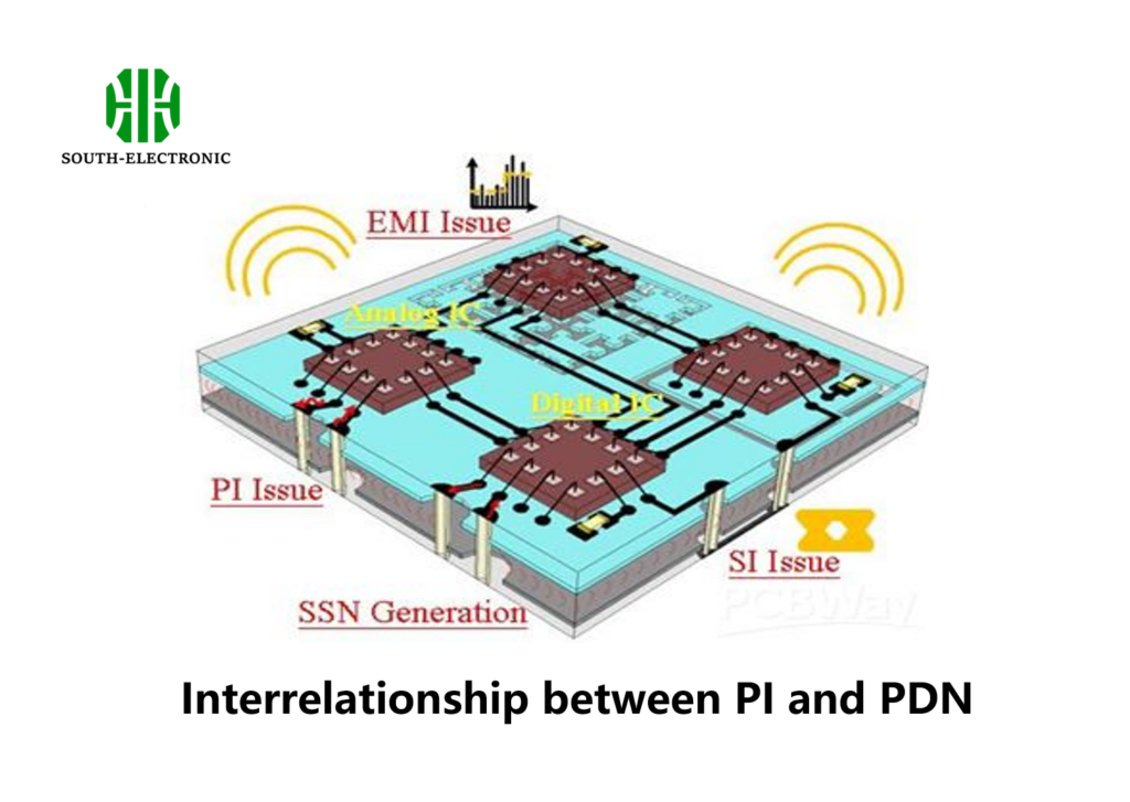
Power Integrity (PI) is directly influenced by the design of the Power Distribution Network (PDN). A poorly designed PDN with high impedance or inadequate decoupling can lead to voltage fluctuations, negatively impacting PI.
To optimize both PI and PDN, engineers must take a holistic approach:
- Simulation Tools: Use simulation tools to analyze PI and PDN performance before finalizing the design.
- Integrated Design Approach: Consider PI and PDN together during the design process, rather than as separate entities.
- Component Placement: Strategically place components to reduce power path lengths and minimize noise.
Emerging Technologies in PI and PDN
As technology advances, new methods and materials are being developed to improve PI and PDN in PCBs. Some emerging trends include:
- Advanced Decoupling Techniques: Using embedded capacitors and advanced materials to improve decoupling performance.
- AI-Driven Design Tools: AI-based tools that optimize PDN and PI during the design phase.
Future high-speed and high-density PCBs will likely require even more sophisticated PI and PDN management techniques. As component density increases and signal speeds rise, the challenges associated with PI and PDN will become even more pronounced.

