
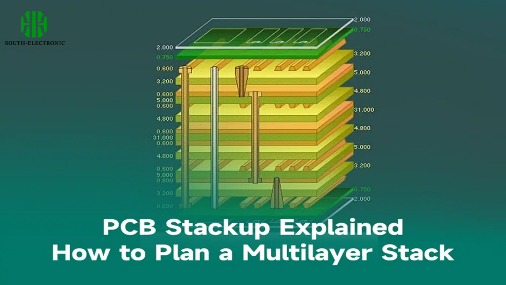
Comment planifier efficacement un empilement de PCB multicouches ?
Les empilements de PCB multicouches impliquent plusieurs couches de composants électroniques et de circuits intégrés dans un matériau non conducteur. La configuration de ces couches joue un rôle essentiel dans les performances de la carte, affectant tout, de l’intégrité du signal à la gestion thermique. Voici les étapes pour planifier un empilement de PCB multicouche :
Voici un aperçu concis et clair des étapes impliquées dans la conception d’un empilement de PCB multicouche :
- Déterminer le nombre de couches : en fonction de la complexité du circuit, décidez du nombre de couches nécessaires pour les signaux, l’alimentation et la terre.
- Sélectionner le matériau : choisissez le matériau de substrat qui répond aux exigences thermiques et électriques de l’application.
- Configuration de l’empilement : concevez la séquence de couches. Généralement, les couches de signaux sont alternées avec des plans d’alimentation ou de masse pour réduire les interférences électromagnétiques (EMI).
- Planification de l’impédance : calculez les exigences d’impédance pour les couches de signaux afin de garantir l’intégrité du signal.
- Intégrité de l’alimentation : Concevez des plans d’alimentation et de masse pour minimiser les chutes de tension et fournir une distribution d’énergie stable.
- Structures via : choisissez les types de via appropriés (traversants, borgnes ou enterrés) en fonction des besoins d’interconnexion entre les couches.
- Gestion thermique : planifiez l’empilement pour faciliter la dissipation de la chaleur, en tenant compte de l’emplacement des vias thermiques si nécessaire.
- Examinez et simulez : utilisez des outils logiciels pour simuler les performances du stackup en termes d’intégrité du signal et de l’alimentation.
- Itérer selon les besoins : modifiez la conception en fonction des résultats de simulation et des tests de prototypes jusqu’à ce que les performances souhaitées soient atteintes.
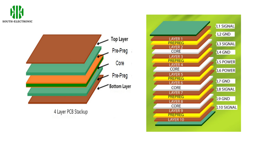
Quelles sont les 4 couches d’empilement de PCB ?
Un empilement de PCB typique à 4 couches comprend :
- Couche supérieure (signal) : contient la majorité des traces de signal.
- Couche de masse interne : agit comme un bouclier et fournit une référence de masse pour la couche supérieure.
- Plan d’alimentation : distribue l’alimentation aux composants du circuit.
- Couche inférieure (signal) : utilisée pour un routage supplémentaire qui ne peut pas être pris en charge sur la couche supérieure.
Cette disposition permet de minimiser les problèmes d’interférences électromagnétiques et d’intégrité du signal, ce qui la rend adaptée aux circuits moyennement complexes.
Quelle est l’épaisseur d’un empilement de PCB à 10 couches ?
L’épaisseur d’un PCB à 10 couches peut varier, mais elle varie généralement d’environ 1,6 mm à 2,4 mm, en fonction des exigences spécifiques de l’application. L’épaisseur de chaque couche et le type de matériau utilisé peuvent affecter l’épaisseur globale de la carte, impactant à la fois les performances et la robustesse physique du PCB.
Erreurs courantes à éviter dans la conception d’empilement de PCB multicouches
Évitez ces erreurs fréquentes pour garantir une conception de PCB de haute qualité :
- Négliger les considérations CEM : Il est essentiel de garantir la conformité aux normes CEM pour éviter les problèmes d’interférence.
- Négliger l’intégrité du signal : une mauvaise planification du routage des traces et de la disposition des couches peut entraîner une dégradation du signal.
- Ignorer les spécifications et les capacités du fabricant : concevez toujours dans les limites de ce que votre fabricant peut produire de manière fiable.
Conclusion
Une planification efficace de l’empilement de PCB multicouches est essentielle pour répondre aux exigences techniques des appareils électroniques modernes. En comprenant et en mettant en œuvre les principes décrits ci-dessus, les concepteurs peuvent garantir que leurs PCB sont optimisés à la fois fonctionnellement et économiquement.

