
Struggling to distinguish PWB from PCB? Confusion between these terms could lead to costly mistakes in electronics projects. Let’s break down their technical differences and historical evolution clearly.
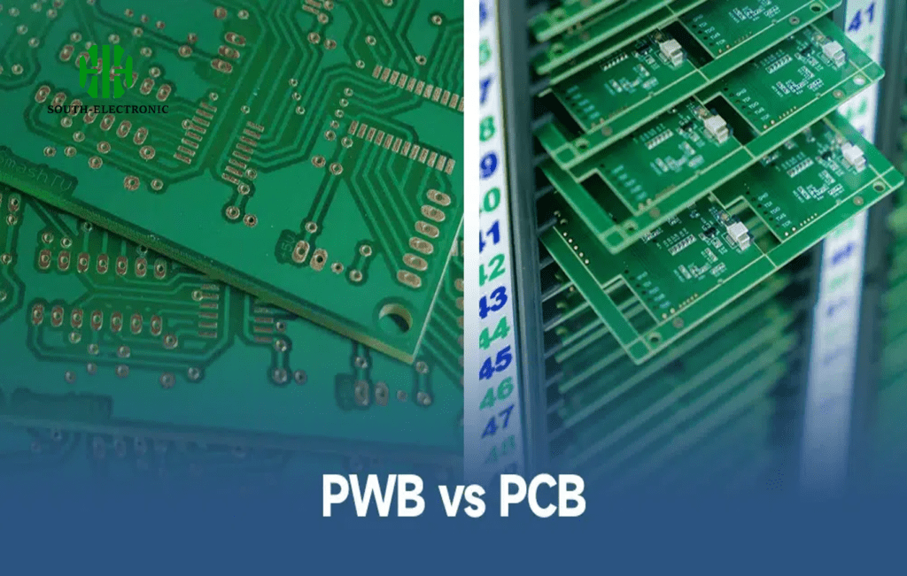
PWBs (Printed Wiring Boards[^1]) are simple single-layer boards for basic circuits, while PCBs (Printed Circuit Boards) handle complex multilayer designs with advanced components. The transition from PWB to PCB reflects evolving industry needs for miniaturization and reliability.
Understanding these differences impacts design choices and manufacturing outcomes. Below, I’ll explore definitions, history, materials, and production processes to clarify when to use each term—and why it matters.
What Is a PWB vs. PCB? Basic Definitions Explained
Ever wondered why two similar acronyms coexist in electronics? Let’s clarify their core meanings to avoid miscommunication in technical discussions.
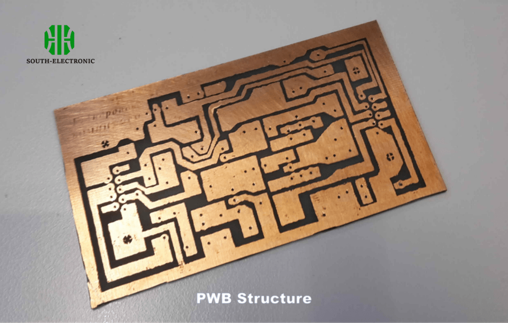
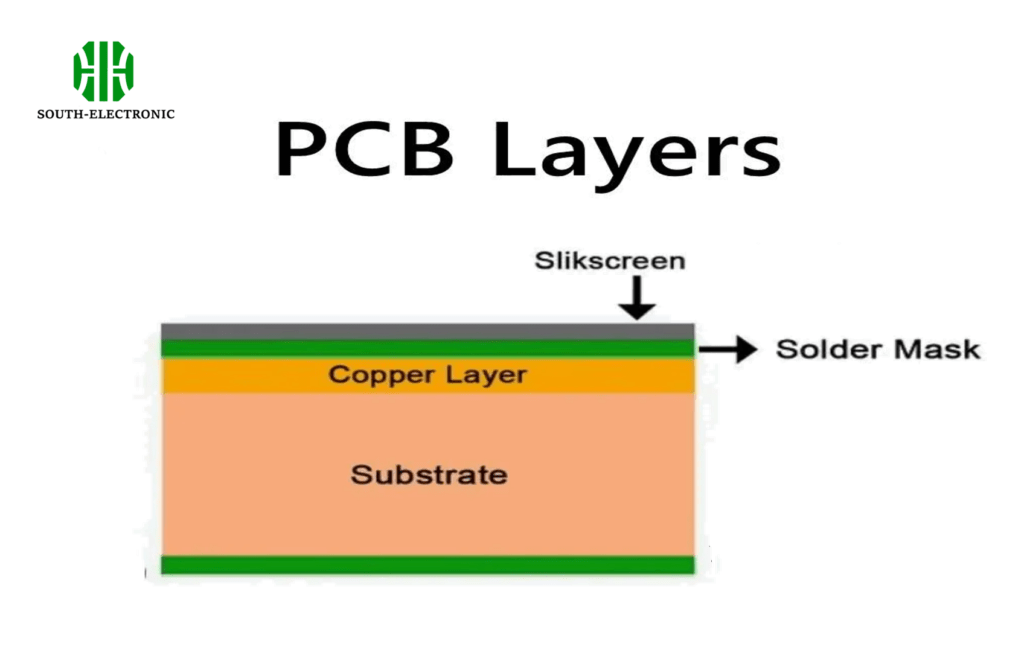
A PWB refers to a board with pre-printed conductive pathways for connecting components. A PCB includes additional features like soldermask, silkscreen, and drilled holes, supporting complex assemblies and automated manufacturing processes.
Breaking Down Terminology
- PWB (Printed Wiring Board):
Primarily used in Japan and older documentation. Focuses on wiring without integrated components. Ideal for low-complexity projects like vintage radios. - PCB (Printed Circuit Board):
Modern term emphasizing full-circuit integration. Supports multi-layer designs[^2] and surface-mount technology (SMT). Common in smartphones and computers.
| Feature | PWB | PCB |
|---|---|---|
| Layer Complexity | Single-layer | Multi-layer |
| Component Integration | External components only | Embedded components |
| Manufacturing Tech | Manual assembly | Automated processes |
| Common Applications | Basic electronics | Advanced devices |
Why Did the Term “PWB” Evolve into “PCB”? A Historical Perspective
Did older engineers use “PWB” while younger ones say “PCB”? The shift reflects technological progress, not just rebranding.
“PWB” originated when boards only provided wiring. As boards began integrating circuits, “PCB” became standard to describe their expanded role in electronic systems.
Timeline of Terminology
- 1940s–1960s:
PWBs dominated in early electronics. Hand-soldered wires connected vacuum tubes and discrete components. - 1970s–1990s:
Integrated circuits (ICs) required denser layouts. “PCB” gained traction as boards evolved beyond simple wiring. - 2000s–Present:
High-density interconnect (HDI) PCBs became industry norm. “PWB” now rarely appears outside legacy contexts.
Are There Differences in Materials and Construction Between PWB and PCB?
Most assume PWBs and PCBs use identical materials. While overlaps exist, their construction complexity separates them.
Both use copper-clad laminates and insulators. However, PCBs employ advanced materials like polyimide for flexibility and FR-4 for heat resistance, while PWBs stick to basic epoxy resins.
Material and Design Comparison
- Base Material:
- PWB: FR-1 (phenolic paper)
- PCB: FR-4 (fiberglass epoxy)
- Conductive Layers:
- PWB: 1 layer
- PCB: 2–20+ layers
- Surface Finish:
- PWB: Often untreated
- PCB: HASL, ENIG, or immersion silver
How Do Manufacturing Processes Differ for PWB and PCB?
Can simpler PWBs reduce production costs? Yes—but modern electronics demand PCB precision.
PWBs involve straightforward etching and drilling.[^3] PCBs require advanced steps like lamination, via plating, and AOI (Automated Optical Inspection) for quality control.
Production Steps Compared
| Process Step | PWB | PCB |
|---|---|---|
| Drilling | Manual or basic CNC | Laser drilling for micro-vias |
| Plating | Rarely used | Electroless copper plating |
| Testing | Visual inspection | Automated electrical testing |
Conclusion
PWBs laid the groundwork, but PCBs dominate modern electronics with superior complexity and reliability. Understanding these terms ensures accurate communication in design and manufacturing.
[^1]: Explore this link to gain a deeper understanding of PWBs, their uses, and how they differ from PCBs in electronics.
[^2]: Learn about multi-layer designs and their critical role in enhancing the functionality and compactness of electronic devices.
[^3]: Explore the benefits of PWBs to understand how they can simplify production and reduce costs in certain applications.


