
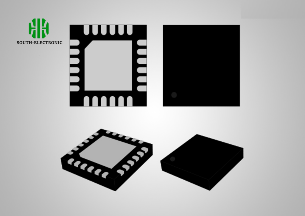
Understanding QFN Packages
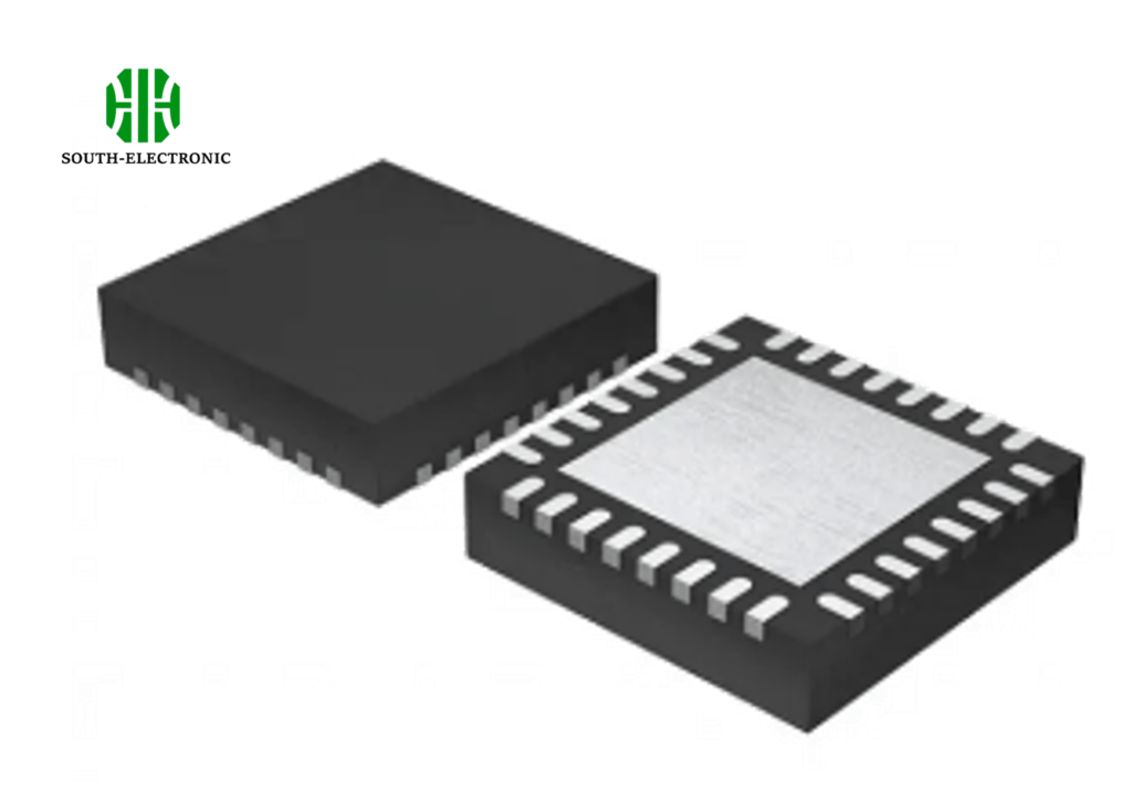
QFN stands for Quad Flat No-Lead. This IC package is known for its lack of protruding leads, which saves PCB space and enhances electrical performance. QFN packages are popular in modern electronics because they are small, have good thermal performance, and are cheap.
Components of QFN Packages
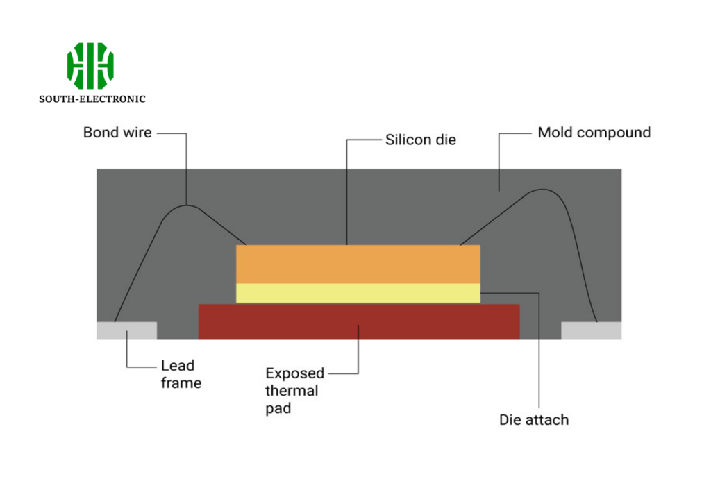
A typical QFN package comprises the following components:
- Lead Frame: Made of a copper alloy with a tin coating, it forms the backbone of the package.
- Silicon Die: The IC’s core component, connected to the lead frame via wire bonding.
- Die Attach: Epoxy material used to secure the die to the exposed pad.
- Mold Compound: Encapsulates the die and wires, protecting them from environmental factors.
Types of QFN Packages
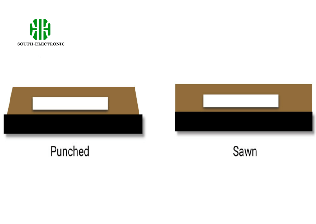
QFN packages come in various forms, distinguished by their molding and singulation processes.
- Punch-Type QFN:In the punch-type method, the package is formed using a single mold cavity. This method is efficient for smaller production volumes.
- Sawn-Type QFN:The sawn-type QFN uses a Mold Array Process (MAP) where multiple packages are created from a single large mold. This is ideal for high-volume production.
Features and Benefits of QFN Packages
QFN packages offer several advantages, making them suitable for various applications:
- Compact Size: Ideal for space-constrained applications.
- Low Inductance: Short bond wires reduce lead inductance, enhancing signal performance.
- Thermal Efficiency: The exposed pad allows for efficient heat dissipation.
- Cost-Effective: The absence of leads and simple construction reduce manufacturing costs.
| Feature | Punch-Type QFN | Sawn-Type QFN |
|---|---|---|
| Molding Method | Single mold cavity | Mold Array Process (MAP) |
| Production Volume | Lower volume | High volume |
| Cost | Moderate | Cost-effective for large quantities |
Applications of QFN Packages
QFN packages are versatile and find applications across various industries:
- Consumer Electronics: Smartphones, tablets, and wearables.
- Automotive Electronics: Engine control units, infotainment systems.
- Industrial Applications: Sensors, controllers.
- Power Management: Power converters, regulators.
Design Considerations for QFN Packages
When designing with QFN packages, several key factors must be considered:
- Footprint Design:The footprint on the PCB must be carefully designed to match the QFN package’s dimensions, ensuring reliable soldering and thermal performance.
- Thermal Management:The exposed pad on the underside of QFN packages plays a crucial role in thermal dissipation. Adequate vias should be placed to facilitate heat transfer away from the IC.
- Inspection and Rework:Due to the package’s leadless nature, inspection can be challenging. Techniques like X-ray inspection are often used to ensure proper solder joint formation.
QFN Package Design Guidelines:
| Design Aspect | Recommendation |
|---|---|
| Footprint Dimensions | Follow datasheet specifications |
| Thermal Vias | Include sufficient vias for heat dissipation |
| Inspection Method | Use X-ray for solder joint inspection |
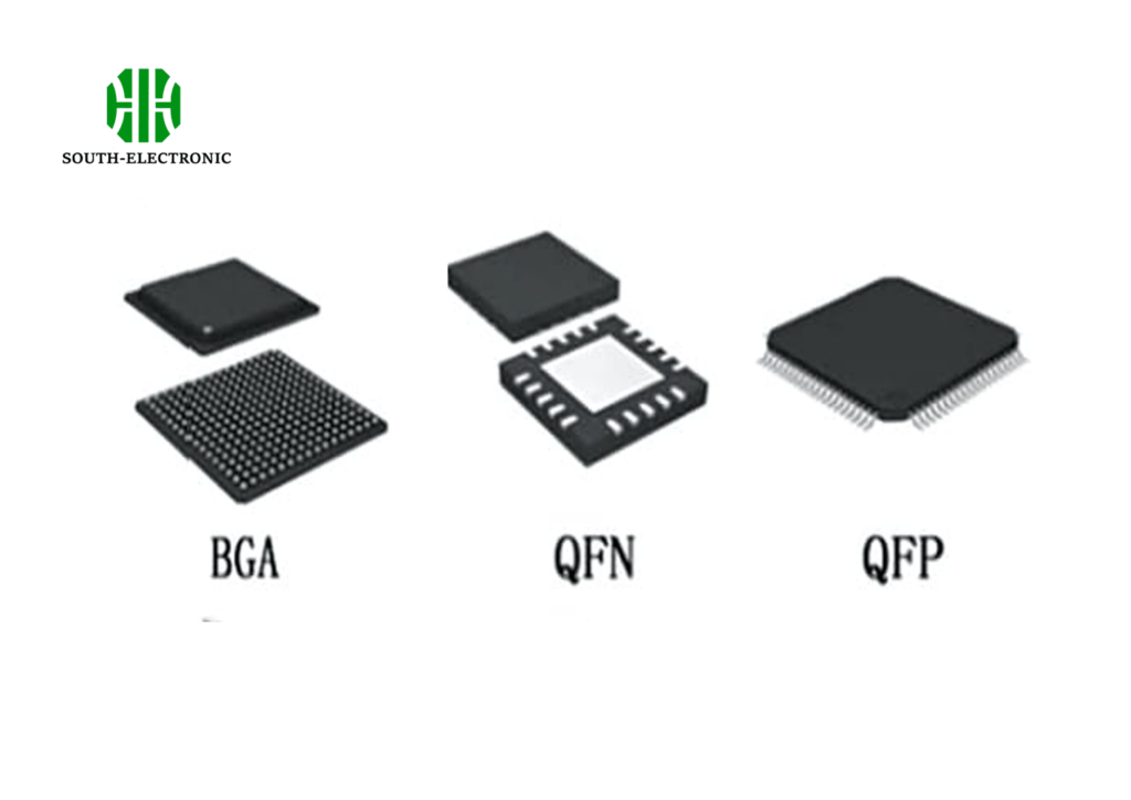
Comparing QFN with Other Packages
QFN vs. QFP
While QFN packages are leadless, Quad Flat Package (QFP) ICs feature leads extending from all four sides. QFPs offer easier inspection but are bulkier and less efficient in terms of space utilization.
QFN vs. BGA
Ball Grid Array (BGA) packages offer excellent thermal performance and are ideal for high pin-count ICs. However, they are more complex and costly to produce compared to QFN packages.
Explore the QFN package process flow, a vital step in semiconductor packaging, offering benefits like enhanced thermal performance and electrical reliability. Discover the different types, including standard QFN, wettable flank QFN, and dual-row QFN, each suited for specific applications. Click here to dive into the advantages and applications of these versatile packages!


