How to Repair Printed Circuit Board?
- Identify and Remove the Damaged Component
- Clean the PCB Area
- Replace the Component
- Test the PCB
- Final Inspection and Cleaning

The detailed steps are as follows:
1.Identify and Remove the Damaged Component
- Identify the faulty component using visual inspection and testing with a multimeter.
- Heat the solder joints of the faulty component using a soldering iron. Apply the iron tip to the joint and wait a few seconds for the solder to melt.
- Remove the solder using a desoldering pump or solder wick. Place the desoldering pump’s nozzle or the solder wick over the molten solder and activate the pump or pull the wick to absorb the solder.
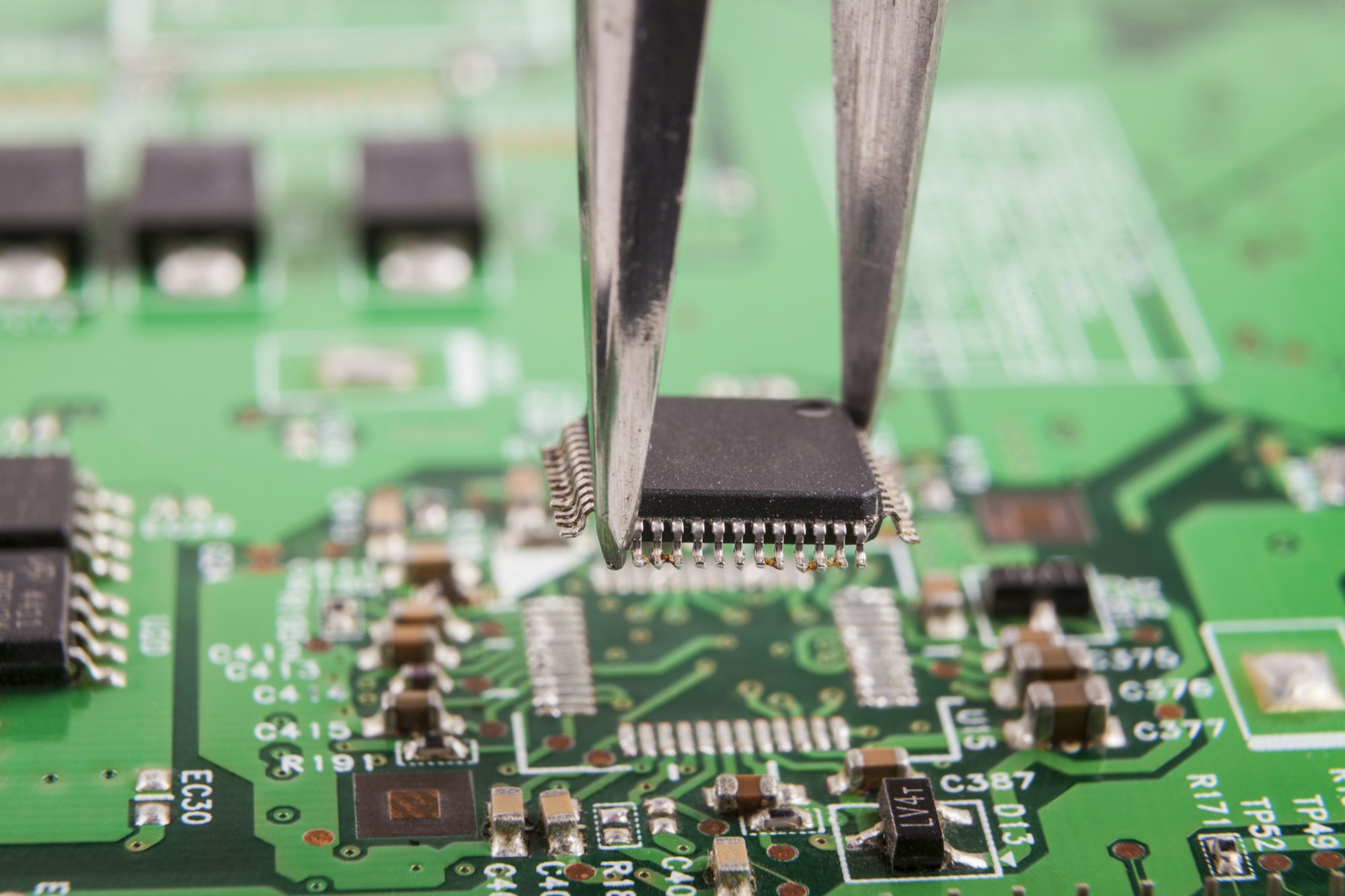
- Carefully lift the component out of its place using tweezers. Be gentle to avoid damaging the PCB pads.
2.Cleaning the PCB
- Use isopropyl alcohol (at least 90% purity) and a soft brush or cotton swab to gently clean the area around the solder pads.
- Remove any residual solder or flux from previous repairs, as these can prevent new solder from adhering properly.
- Allow the PCB to dry completely before proceeding to the next steps.
3.Repairing or Replacing Components
- Position the new component precisely where the old one was located. Use tweezers to place it correctly, aligning all pins with the corresponding pads.
- Apply flux to the pads to promote better solder flow.
- Solder each pin of the new component. Touch the soldering iron tip to the pad and the pin, and feed a small amount of solder into the joint. Remove the iron and allow the solder to cool without moving the component.
- Inspect each solder joint under a magnifying glass or microscope to ensure it is smooth and adequately covers the pad without bridging to other pins.
4.Testing the PCB
- Power up the PCB carefully, monitoring for any signs of overheating, smoke, or unusual smells which could indicate a problem.
- Use a multimeter to check for continuity, ensuring that each replaced component is properly connected without short circuits.
- Test the functionality of the circuit by simulating its normal operating conditions and measuring the output. Adjustments may be necessary if the circuit does not perform as expected.
5.Final Inspection and Cleaning
- Clean the PCB again with isopropyl alcohol to remove any flux residue left from soldering.
- Inspect the entire board for any potential issues that could have been overlooked, such as small solder splashes or loose components.
- Test the board one final time to confirm everything is fully functional.
What are the common faults of PCB?

When it comes to PCB failures, there are a bunch of different things that can go wrong. You might have physical damage from dropping or hitting the board, or you could have thermal damage from too much heat. Moisture can cause corrosion, and chemicals can eat away at the materials on the board. Electrical problems like electrical overstress (EOS) and electrostatic discharge (ESD) can fry your components. If you don’t know what you’re doing when you solder, you can mess up your board, and if your board gets dirty, that can mess it up too. A lot of times, these problems are made worse by bad PCB design that doesn’t take into account the physical and electrical stresses the board will face.
What are the risks of PCB repair?
Repairing printed circuit boards (PCBs) can be risky due to several factors. The complexity and miniaturization of modern PCBs make them susceptible to damage from excessive heat during soldering. The use of incorrect tools or materials can lead to further damage or failure of the PCB. Additionally, exposure to toxic chemicals, such as those found in some solder and cleaning agents, poses health risks. Furthermore, improper handling can lead to electrostatic discharge (ESD), which can destroy sensitive components.

When repairing printed circuit boards (PCBs), several essential safety measures are crucial to ensure both the integrity of the PCB and the safety of the technician:
- Wearing appropriate personal protective equipment (PPE) such as gloves and goggles is important to protect against chemical exposure and physical injuries.
- Using ESD (Electrostatic Discharge) protective gear, including wrist straps and ESD mats, helps prevent damage to sensitive electronic components.
- It’s also vital to work in a well-ventilated area to avoid inhalation of toxic fumes from soldering and cleaning chemicals.
- Using the correct tools and following manufacturer guidelines can prevent damage to the PCB.
- Finally, ensuring that all equipment is properly grounded can help avoid electrical shocks and fires.


