
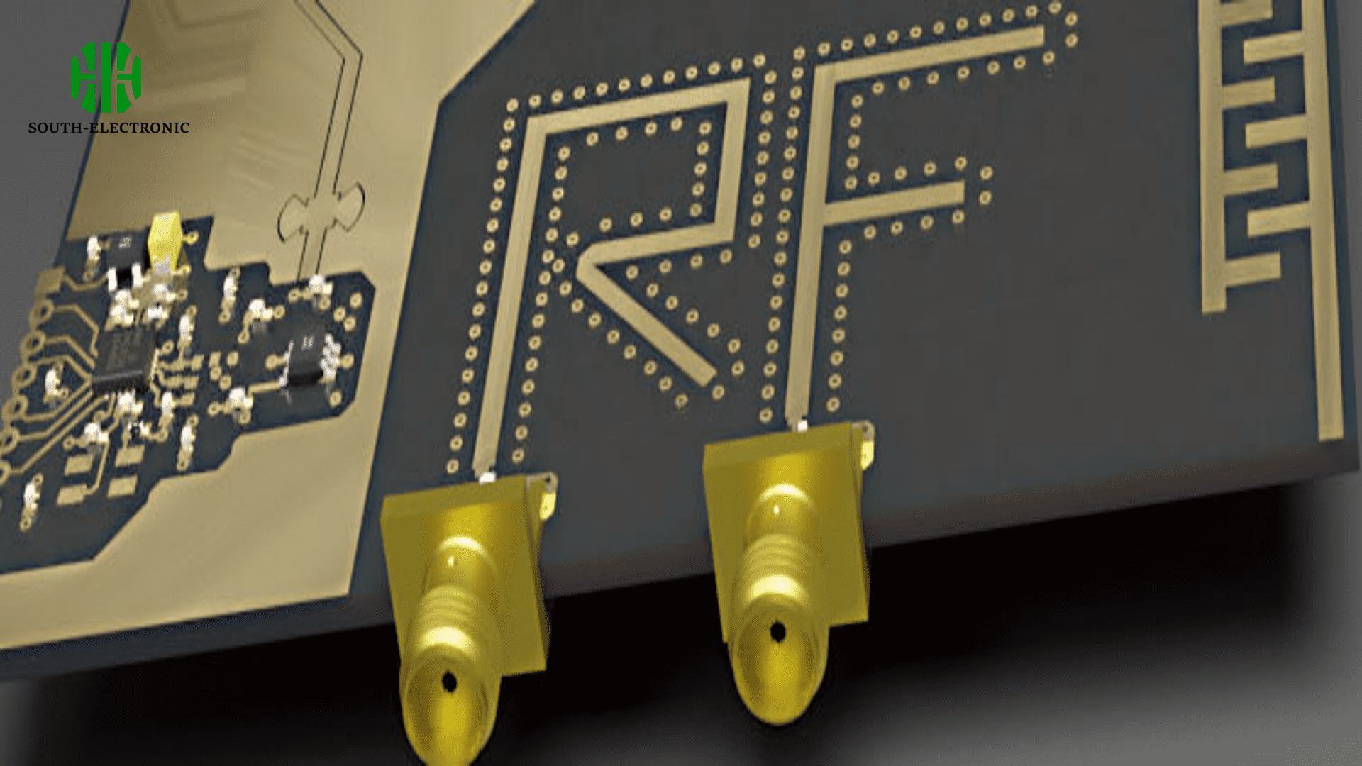
RF PCB (Radio Frequency Printed Circuit Board) design is a specialized area within PCB design that deals with high-frequency signals. This type of design requires a good understanding of RF principles, materials, and layout techniques.
Understanding RF Signal Behavior
High-frequency signals do some weird stuff. They don’t just flow through a conductor like a nice, predictable DC signal. They have all kinds of strange behaviors, like skin effect, dielectric loss, and electromagnetic interference. If you want to design a good RF PCB, you need to understand these behaviors.
- Skin Effect:At high frequencies, current tends to flow on the surface of conductors, known as the skin effect. This reduces the effective cross-sectional area and increases resistance.
- Dielectric Loss:Dielectric materials used in PCBs can cause signal loss at high frequencies. Choosing low-loss materials is essential for maintaining signal integrity.
- Electromagnetic interference (EMI): disruption of electronic signals caused by external electromagnetic fields. In RF PCB design, minimizing EMI is crucial to ensure signal integrity and prevent noise, which can degrade the performance of high-frequency circuits.
Choosing the Right Materials
Substrate Material
The substrate material should have low dielectric loss and stable dielectric constant. Common materials include FR4, Rogers, and Teflon.
| Material | Dielectric Constant | Loss Tangent |
|---|---|---|
| FR4 | 4.5 | 0.02 |
| Rogers 4350 | 3.48 | 0.0037 |
| Teflon | 2.1 | 0.0002 |
Conductive Materials
Copper is the most commonly used conductor because it has excellent electrical properties. However, at very high frequencies, you might use silver or gold plating to reduce loss.
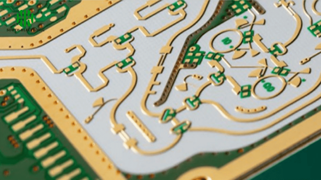
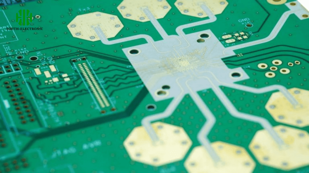
Best Practices for Layout and Signal Integrity
Trace Width and Spacing
Calculate trace widths and spacing using impedance control to ensure signal integrity. Use coplanar waveguide or microstrip lines for high-frequency signals.
| Trace Type | Impedance (Ohms) | Application |
|---|---|---|
| Microstrip Line | 50 | General RF Signals |
| Coplanar Waveguide | 50 | High-density Routing |
Ground Planes
Use continuous ground planes to minimize noise and provide a return path for signals.
Planning and Simulation
Use simulation tools to analyze signal integrity, electromagnetic interference, and thermal performance. Before finalizing your design, thorough planning and simulation are essential to ensure performance and reliability.
Prototyping and Testing
Build prototypes and test them under real-world conditions to identify and resolve any issues before mass production.
Incorrect Impedance Matching
Incorrect Impedance Matching:Ensure that all signal paths are properly impedance-matched to prevent signal reflection and loss.
Poor Component Placement:Place components in a way that minimizes signal path length and avoids crosstalk.
When you start designing RF PCBs, you need to know how high-frequency signals act, choose the right materials, use special tools, and follow best practices for layout and signal integrity. You have to plan, simulate, and test to make sure your RF PCB works well and is reliable. This guide will help you learn how to design RF PCBs and make circuits that work well and are reliable for high-frequency applications.

