
What are the wiring priority requirements?
(a) Priority for key signal lines: power supply, analog small signals, high-speed signals, clock signals and synchronization signals are prioritized.
(b) Wiring density priority principle: Start wiring from the device with the most complex connection relationship on the single board. Start wiring from the area with the densest wiring on the single board.
(c) Notes on key signal processing: Try to provide dedicated wiring layers for key signals such as clock signals, high-frequency signals, and sensitive signals, and ensure their minimum loop area. If necessary, shielding and increasing safety spacing should be adopted to ensure signal quality.
(d) Networks with impedance control requirements should be arranged on the impedance control layer, and their signals must not be split across.
Wiring crosstalk control skills
(a) 3W principle explanation The distance between lines should be kept 3 times the line width. In order to reduce crosstalk between lines, the line spacing should be large enough. If the line center distance is not less than 3 times the line width, 70% of the electric fields between lines can be kept from interfering with each other, which is called the 3W rule.

(b) Crosstalk control: Crosstalk refers to the mutual interference between different networks on a PCB caused by long parallel wiring, mainly due to the distributed capacitance and distributed inductance between parallel lines. The main measures to overcome crosstalk are:
-
Increase the spacing between parallel wiring and follow the 3W rule;
-
Insert grounded isolation wires between parallel lines;
-
Reduce the distance between the wiring layer and the ground plane.
What are the general rules for wiring?
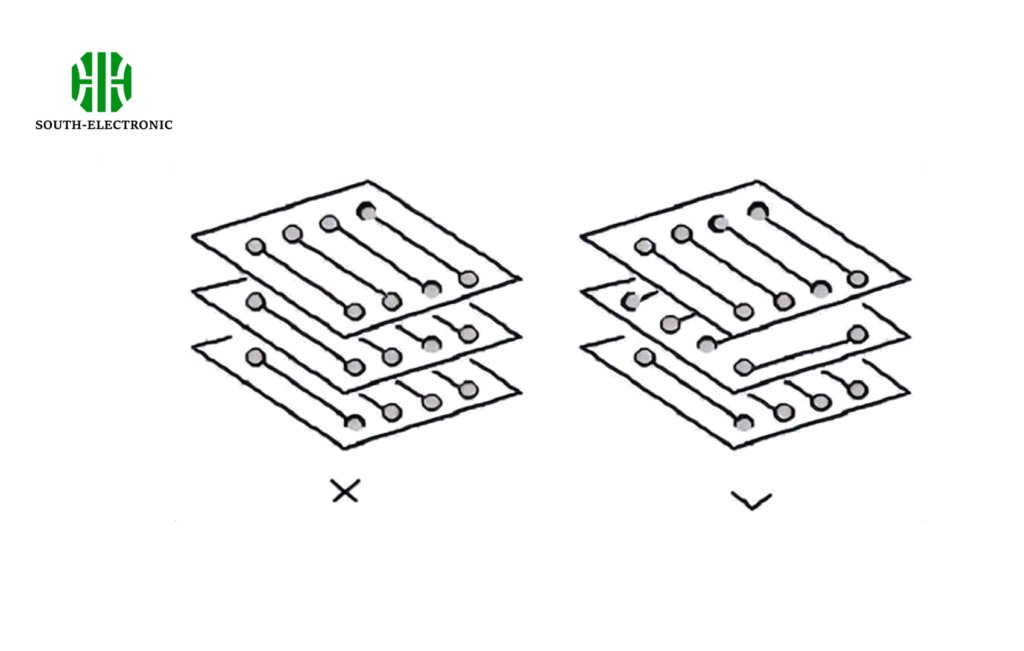
(a) The routing directions of adjacent planes to be orthogonal. Avoid running different signal lines in the same direction on adjacent layers to reduce unnecessary inter-layer crosstalk; when this situation is difficult to avoid due to board structure limitations (such as some backplanes), especially when the signal rate is high, consider using ground planes to isolate each wiring layer and using ground signal lines to isolate each signal line.
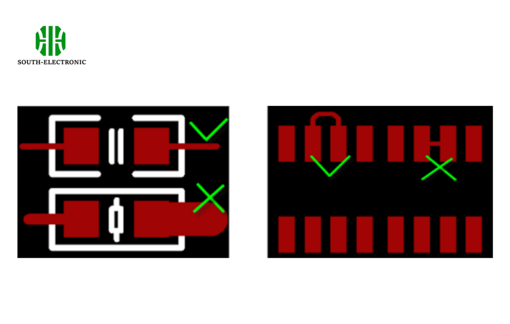
(b) The routing of small discrete devices must be symmetrical. The leads of SMT pads with relatively close spacing should be connected from the outside of the pads. Direct connection in the middle of the pads is not allowed.
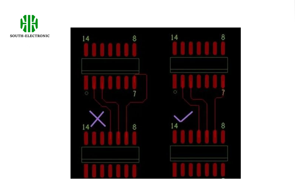
(c) The minimum loop rule, that is, the loop area formed by the signal line and its loop should be as small as possible. The smaller the loop area, the less external radiation and the less external interference.
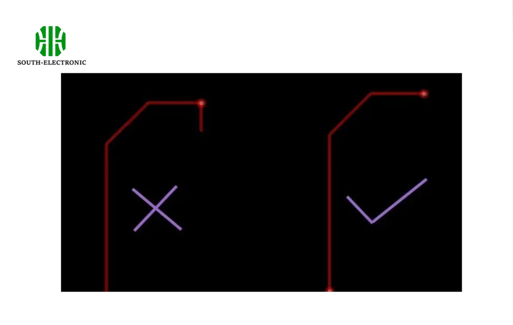
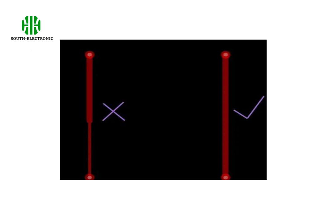
(d) No STUB is allowed in the routing.
(e) The wiring width of the same network should be consistent. The change of line width will cause uneven characteristic impedance of the line, and reflection will occur when the transmission speed is high. Under certain conditions, such as the similar structure of the connector lead wire and the lead wire of the BGA package, the change of line width may not be avoided due to the small spacing. The effective length of the inconsistent part in the middle should be minimized.
(f) Prevent the signal line from forming self-loops between different layers. This problem is easy to occur in multi-layer board design, and self-loops will cause radiation interference.
(g) Sharp angles and right angles should be avoided in PCB design, which will generate unnecessary radiation and poor PCB production process performance.
Conclusion
Prioritize key signals (power, clock, etc.), use the 3W principle and isolation lines to control crosstalk; follow the orthogonal wiring of adjacent layers, maintain the minimum loop, avoid right angles and self-loops, ensure consistent line width, and prevent signal reflection and interference.

