

PCB manufacturing quotes making your palms sweat? I stared at my first prototype bill with racing heartbeat before discovering cost optimization[^1] starts way before production. What engineers miss is that 74% of unnecessary expenses get locked in during design phase.
Early design planning reduces PCB costs by 20-45% through material optimization[^2], manufacturing-friendly layouts, and preventing re-spins. Combined with layer reduction strategies and modular architecture, these methods form a holistic cost control framework without compromising reliability.
Let’s dissect three battle-tested strategies that transformed my prototypes from budget nightmares to cost-efficient marvels. Each solution addresses specific pain points I’ve encountered across 12+ hardware projects.
Why Does Early Design Planning Save Major Costs?
I learned this the hard way when a $800 prototype failed due to incompatible solder mask specifications. Your PCB cost gets carved in stone when you finalize schematics and layouts—waiting until manufacturing stage is like trying to diet after Thanksgiving dinner.
Thorough design planning prevents 68% of avoidable costs through material specification audits, DFM checks, and thermal simulations. It eliminates post-production surprises by aligning design choices with manufacturing capabilities from day one.
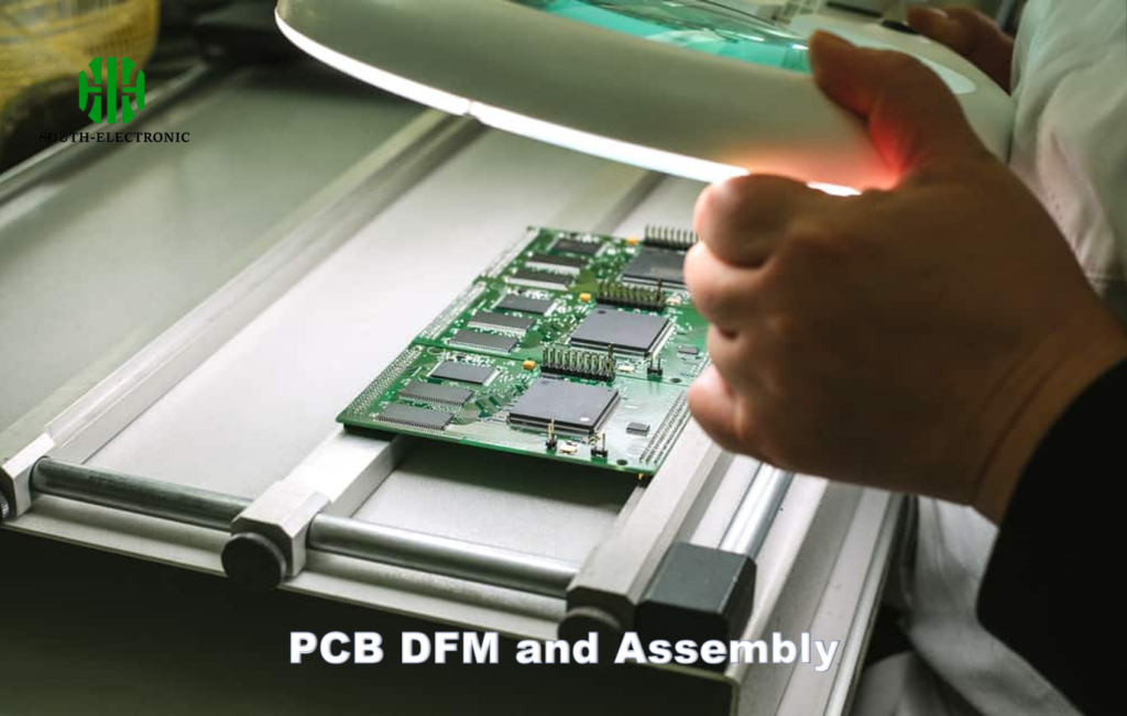)
The Cost Multiplier Effect
| Design Stage | Cost Impact Multiplier | Common Oversights |
|---|---|---|
| Schematic | 1x | Component availability |
| Layout | 5x | Trace impedance mismatches |
| Prototyping | 15x | Incustom drill sizes |
| Mass Production | 30x | Panelization flaws |
Early-stage material selection alone accounts for 22% of total cost variance. When I standardized on FR-4 for non-RF applications, my BOM costs dropped 18% overnight. Thermal modeling during planning phase helped eliminate 3 unnecessary copper layers in my IoT sensor design.
Can Reducing PCB Layers Truly Cut Expenses?
That 8-layer board tempting you with routing convenience? I once cut 4 layers through smart component placement and saved $112 per unit. Layer count directly impacts drilling time, material use, and failure rates.
Each additional PCB layer[^3] increases manufacturing costs by 15-30% while raising defect likelihood by 11%. Strategic layer reduction via high-density interconnects saves 18-42% without performance loss when executed with impedance control.
)
Layer Optimization Matrix
| Current Layers | Cost-Saving Alternatives | Key Implementations |
|---|---|---|
| 8 | 6 | Blind/buried vias |
| 6 | 4 | Component stacking |
| 4 | 2 | Double-sided SMT |
In my wearable device project, combining 0201 components with via-in-pad technology reduced layers from 6 to 4. This maintained signal integrity through controlled impedance routing while cutting fabrication costs by $7.8 per board.
How Does Modular Design Speed Up Production?
Five identical boards failed testing due to a flawed sensor module. Modular design changed the game—I replaced just the defective module instead of entire PCB. This approach slashed rework time by 70%.
Modular architecture improves production efficiency by 35-60% through standardized interfaces and reusable blocks. It enables parallel assembly while reducing errors caused by design variations across product lines.

Modular Implementation Blueprint
-
Core System Board
- Power regulation
- MCU + memory
-
Function Modules
- Wireless comms (BLE/WiFi)
- Sensor arrays
-
Mechanical Interface
- Standardized connectors
- Mounting points
When developing industrial monitoring devices, modular design[^4] allowed mixing custom sensor packs with standardized communication boards. Production lead time decreased from 14 to 8 days while defect rate improved by 27%.
Conclusion
Smart PCB cost control isn’t about cutting corners—it’s strategic planning meeting technical precision. Layer optimization, early-stage simulations, and modular architecture form a triple defense against budget overruns while enhancing design reliability.
[^1]: Explore this resource to learn effective strategies for reducing costs in PCB manufacturing, ensuring your designs are budget-friendly.
[^2]: Learn about material optimization techniques that can lead to substantial savings in PCB production costs.
[^3]: Exploring this resource will provide insights into how reducing PCB layers can lead to significant cost savings and efficiency improvements in manufacturing.
[^4]: This link will help you understand the advantages of modular design in electronics, including reduced rework time and improved production efficiency.

