
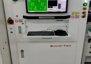
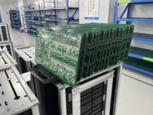
PCB Fabrication Assembly
South-Electronic
Choose South-Electronic for top-notch quality, dependability, and great value in your PCB manufacturing needs. See the difference with our full-service PCB Fabrication Assembly services — from initial design to finished product, we guarantee accuracy, durability, and compliance with the highest industry standards.
Your Premier Partner in PCB Fabrication and Assembly
Welcome to South-Electronic. We provide top-notch PCB Fabrication Assembly services that are known for their accuracy and reliability.
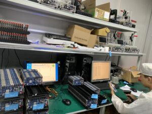
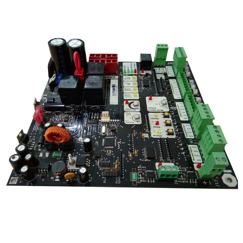
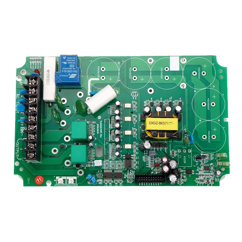
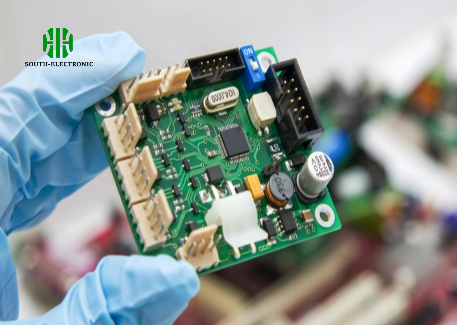
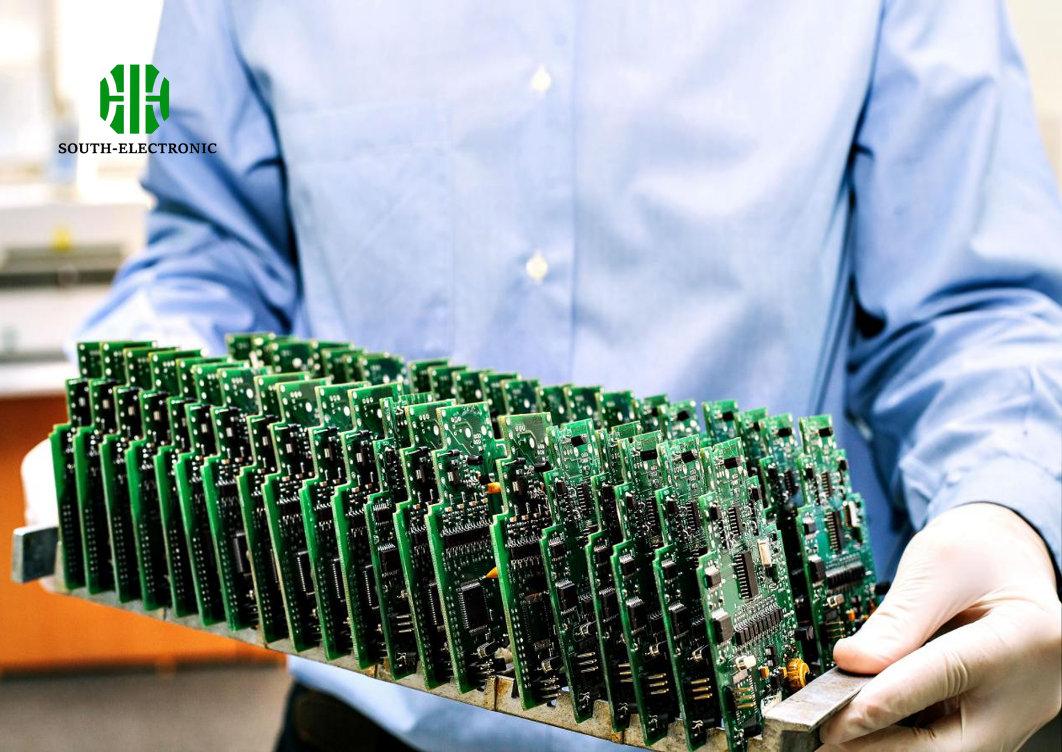
Our PCB assemblies are perfect for a wide range of applications. We offer rigid, flex, and multi-layer PCBs that can be customized to meet your specific electronic needs. Whether you need to improve the efficiency of your consumer electronics or ensure that your industrial controls operate reliably, our PCB Fabrication Assembly services are designed to deliver efficiency and precision. When you choose South-Electronic, you can count on consistent quality and innovation for your electronic projects. Our PCB assemblies will enhance the performance and reliability of your devices. Trust us to provide excellence and creativity for your industry.
Why Choose South-Electronic?
-
Flexibility in Ordering
You get exactly what you need, no matter the order size.
Whether it’s a single piece or thousands, we’re ready to fulfill your order with the same dedication to quality and precision -
Comprehensive Service
Get everything you need in one place.
From design to delivery, our advanced technology and manufacturing capabilities guarantee that your order is completed to the highest standards. -
Fast Delivery
You stay on schedule with our fast turnaround times.
Our streamlined production ensures fast turnaround times, so you get your products when you need them, without delays. -
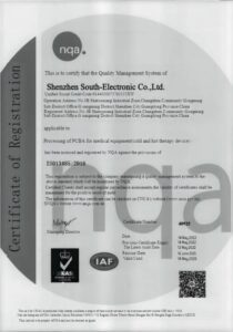
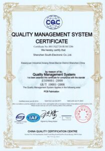
Guaranteed Satisfaction
You’ll appreciate the confidence that comes with working with an ISO9001 certified company.
We prioritize clear, transparent communication and hold ourselves to the highest standards, ensuring that your 8-layer PCBs not only meet but exceed your expectations for performance, durability, and precision.
Related Project We had Done
Customer Reviews
Common Questions
Most Popular Questions
Send us a message
The more detailed you fill out, the faster we can move to the next step.


The Complete Guide For PCB Fabrication Assembly
Contents
Chapter 1
Introduction to PCB Fabrication Assembly
PCB Fabrication and Assembly is a critical process in the world of electronics manufacturing. PCBs are the backbone of most electronic devices, providing mechanical support and electrical connections between components. Here is an overview of the importance and intricacies of PCB fabrication and assembly:
What is PCB Fabrication?
PCB fabrication is the process of creating the physical structure of the circuit board. This involves several steps, from design layout to the finished product:
- Design Layout: Engineers design a schematic, which is then converted into a digital layout using specialized CAD software. This layout includes component placement and the routing of electrical connections, known as traces.
- Material Selection: The base material, typically a fiberglass-reinforced epoxy laminate (FR-4), is chosen for its durability and insulating properties. Copper is used for conducting paths, along with other elements tailored to specific device needs.
- Patterning and Etching: The design is printed onto the board, and unwanted copper is etched away, leaving only the desired circuit paths.
- Drilling and Plating: Holes are drilled for component leads and vias, which are plated to ensure conductive paths between different layers of the PCB.
- Solder Mask and Silkscreen: A solder mask is applied to protect copper traces and prevent soldering errors. The silkscreen layer is added to print labels and reference indicators on the PCB.
What is PCB Assembly?
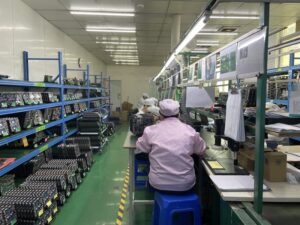
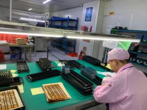
PCB assembly is the process of placing and soldering electronic components onto the fabricated PCB. This includes:
- Component Placement: Automated machines accurately place components onto the PCB according to the design specifications. This can include resistors, capacitors, integrated circuits (ICs), and more.
- Soldering: Various soldering techniques are used to secure the components in place and establish electrical connections. Surface-mount technology (SMT) and through-hole technology (THT) are common methods.
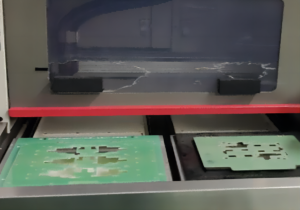
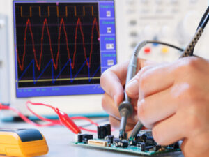
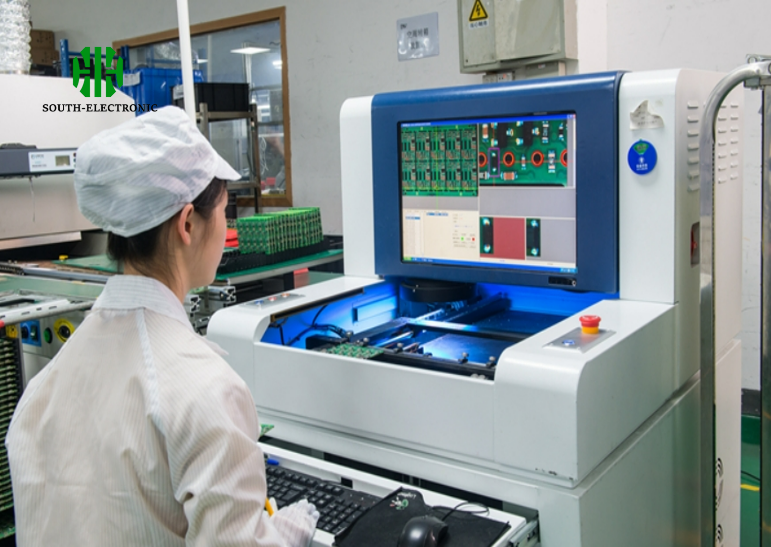
- Inspection and Testing: After assembly, PCBs undergo thorough inspection and testing to ensure they function correctly and meet quality standards. This includes visual inspections, automated Optical Inspection (AOI), and functional tests.
Importance in Electronics Manufacturing
PCBs are essential in all electronic devices, from smartphones and computers to medical devices and automotive electronics. The precision and efficiency of PCB fabrication and assembly directly impact the performance, reliability, and lifespan of the final electronic product.
The demand for smaller, more efficient, and more complex electronic devices continues to grow, making PCB fabrication and assembly more important than ever. As the foundation for technological innovation, understanding and investing in advanced PCB processes is critical for any company looking to stay competitive in the electronics market. This guide aims to provide you with a comprehensive understanding of these processes, ensuring your journey in electronics manufacturing is informed and successful.
Chapter 2
Understanding PCB Types and Uses
PCBs come in different types, each designed to meet specific requirements and challenges posed by different electronic applications. Understanding these types and their uses is crucial for selecting the right PCB for your project. Here’s a detailed look at the different types of PCBs and their applications across industries:
Types of PCBs
Single-Sided PCB:
- Structure: These PCBs have a single layer of substrate with conductive copper on one side. Components are mounted on one side, and the circuit’s traces are etched on the other.
- Applications: Used in simple, low-density designs such as calculators, power supplies, and certain home appliances due to their cost-effectiveness and simplicity.
Double-Sided PCB:
- Structure: Feature a substrate layer with copper layers on both sides. Components can be mounted on either side with connections established through holes (vias).
- Applications: Suitable for more complex circuits than single-sided PCBs. Common in vehicle dashboards, industrial instrumentation, and lighting systems.
Multilayer PCB:
- Structure: Consist of three or more conductive layers separated by insulating material. These PCBs allow for complex circuit designs with multiple layers stacked on top of each other.
- Applications: Ideal for highly sophisticated devices like smartphones, data storage solutions, medical equipment, and satellite systems due to their ability to support high component density and intricate designs.
Rigid PCB:
- Structure: Constructed from a solid substrate that prevents the board from bending. They are durable and provide structural support for components.
- Applications: Examples include computer motherboards, hard drives, and televisions, where a stable and non-flexible platform is necessary.
Flexible PCBs (Flex PCBs):
- Structure: Made of materials that allow the board to bend or flex, typically using a polyester or polyimide substrate.
- Applications: Used in applications requiring flexibility such as wearable electronics, cameras, and various medical devices, allowing the circuit to conform to different shapes.
Rigid-Flex PCB:
- Structure: Combine elements of both rigid and flexible PCBs, featuring layers that can be both flexible and rigid.
- Applications: Provide versatile solutions in complex systems like aerospace applications, military systems, and advanced consumer electronics, where space and weight are limited.
Applications Across Industries
Consumer Electronics: In devices like smartphones, tablets, and home appliances, a mixture of multilayer, rigid, and flex PCBs are used to accommodate advanced features while optimizing space and functionality.
- Automotive Industry: PCBs are essential for managing vehicle electronics including navigation, control systems, and infotainment, requiring durable multilayer and rigid PCBs.
- Medical Devices: Miniaturization and reliability are key, with many medical equipment employing flexible and rigid-flex PCBs to accommodate compact and portable designs, such as pacemakers and imaging equipment.
- Industrial Equipment: Double-sided and multilayer PCBs are commonly used in control systems, robotics, and machinery to support higher-performance requirements and robust operation.
- Aerospace and Defense: These sectors often use advanced multilayer and rigid-flex PCBs to handle extreme conditions and rigorous performance standards, essential in satellite communications and military hardware.
- Selecting the appropriate type of PCB based on the application and industry requirements is vital for ensuring optimal performance, cost-effectiveness, and reliability in electronic designs. Understanding these PCB types and their diverse applications empowers engineers and designers to innovate and enhance technology across various domains.
Chapter 3
Key Components in PCB Fabrication
PCB fabrication is a complex process that involves many different materials and components. Each of these components plays a critical role in determining the performance, reliability, and manufacturability of the final product. Understanding these materials is essential for designing effective and efficient PCBs. In this article, we will take a detailed look at some of the key components used in PCB fabrication.
1. Substrates
The substrate is the base material of a PCB. It provides the necessary support structure for all the other components. The most commonly used substrate material is FR-4, which is a fiberglass-reinforced epoxy laminate. FR-4 is popular because it has excellent electrical insulation properties, mechanical strength, and is cost-effective. However, for high-frequency applications, you might need to use PTFE substrates, which have superior electrical properties at microwave frequencies. For applications that require enhanced thermal dissipation, you might need to use metal-core substrates.
2. Copper Layers
Copper foils are laminated onto the substrate to form conductive pathways or traces. The thickness of the copper can vary depending on the current-carrying requirements of the PCB. Copper thickness is typically measured in ounces per square foot. Common thicknesses include 1 oz, 2 oz, and 3 oz. Thicker copper is used in PCBs for power electronics to handle high currents, whereas thinner copper is sufficient for signal processing.
3. Laminates
Laminates consist of layers of the substrate material bonded with layers of copper foil. Rigid laminates provide a sturdy backing for components and are mainly used in non-flexible PCBs. Flexible laminates use materials like polyimide to allow the PCB to flex without damaging the conductors.
4. Prepreg
Prepreg is a composite material impregnated with a resin system. It is used as an adhesive and insulating layer between laminate layers in multilayer PCBs. Prepreg provides the necessary bond strength between layers. It is available in different thicknesses and has varying resin content to meet specific thermal behaviors.
5. Solder Mask
The solder mask is a protective layer that covers the copper traces to prevent short circuits, soldering errors, and environmental damage. It is usually a polymer-based coating applied over the copper layers of the PCB. Solder masks come in different colors, with green being the most common. However, alternatives like red, blue, and black are also available for aesthetic purposes or each version’s specific properties.
6. Silkscreen
The silkscreen is a layer of ink traces that is printed on the PCB for labeling component placements, warnings, and symbols. It is usually a non-conductive epoxy ink that stands out against the solder mask for easy readability.
7. Vias
Vias are the conductive paths drilled through the substrate to connect copper traces on different layers of the PCB. There are different types of vias, including through-hole vias, blind vias, and buried vias. Through-hole vias extend from the top to the bottom layer. Blind vias connect external layers with one or more internal layers without going through the entire board. Buried vias connect internal layers only, facilitating more complex multilayer configurations.
8. Surface Finishes
Surface finishes are applied to copper traces to prevent oxidation and ensure good solderability. There are several different types of surface finishes, including HASL (Hot Air Solder Leveling) and ENIG (Electroless Nickel/Immersion Gold). HASL is economical and provides good solderability. ENIG offers a smooth surface and excellent shelf life. It is preferred for high-quality and fine-pitch components.
Understanding these components is vital for engineers and designers to ensure that the PCB design is suitable for its intended application, reliable in performance, and cost-efficient to manufacture. Each component enhances specific attributes of the PCB and influences the overall functionality and quality of the electronic device.
Chapter 4
The PCB Design Process
Creating a PCB involves a series of steps that turn an initial electronic circuit concept into a manufacturable and functional board. This process relies heavily on software tools, design rules, and manufacturability considerations. Here’s a detailed guide to designing PCBs:
Step 1: Define Requirements and Specifications
- Objective: Clearly define the functional and performance requirements of the PCB.
- Considerations: Determine the size, shape, and environment in which the PCB will operate. Consider factors like power, signal types, and component placement.
Step 2: Schematic Capture
Software Tools: Use Electronic Design Automation (EDA) tools like Eagle, KiCad, Altium Designer, or OrCAD.
Process:
- Create a schematic diagram that represents circuit components symbolically and their interconnections.
- Ensure that all electronic components are correctly specified, including values and types.
Step 3: Component Placement
- Objective: Optimize layout for electrical performance and ease of assembly.
- Considerations: Place components based on signal flow and proximity to related components. Critical components like microprocessors should be centrally located. Consider thermal management and mechanical constraints.
Step 4: Routing the Traces
Software Tools: Use PCB layout tools integrated within the EDA software to define electric paths, or traces, connecting components.
Design Rules:
- Ensure adequate spacing to prevent short circuits and signal interference.
- Use appropriate trace widths based on current-carrying capacity and impedance requirements.
Techniques: Implement power and ground planes to minimize noise and enhance performance. Use automatic or manual routing for complex layouts.
Step 5: Design Rule Check (DRC)
Purpose: Validate the design according to predefined design rules to ensure manufacturability and functionality.
Process:
- Run DRC features in EDA tools to check for violations, such as incorrect trace spacing, minimal vias, and component overlap.
- Adjust and correct any errors reported during the check.
Step 6: Generate Gerber Files
- Objective: Create standardized output files that represent the PCB design for manufacturing.
- Files Included: Separate files for each copper layer, solder mask, silkscreen, and drill holes. These files are essential for the PCB fabrication process.
Step 7: Consider Manufacturability (DFM)
Objective: Ensure the design is feasible for cost-effective and high-quality manufacturing.
Considerations:
- Work with manufacturers early to understand their capabilities and constraints.
- Include clear annotations and notes on assembly requirements.
- Choose surface finishes and solder mask colors based on availability and application needs.
Step 8: Simulation and Testing
- Objective: Predict the performance of the PCB under various conditions using simulation tools.
- Process: Use software to simulate thermal, electrical, and mechanical behavior, verifying stability and signal integrity.
Step 9: Prototype and Validation
- Objective: Build and test a prototype to verify that it meets all design specifications and functional requirements.
- Process: Conduct structured testing to identify performance discrepancies and make necessary refinements in the design for improvement.
Considerations for Manufacturability
- Collaborate with Manufacturers: Engage with your chosen manufacturer during the design phase to align design capabilities with manufacturing capabilities.
- Minimize Complexity: Choose the simplest design that meets the application’s requirements to reduce costs and increase reliability.
- Plan for Scalability: Design with future production scales in mind to ensure the layout can be manufactured in larger quantities without redesign.
Designing a PCB is a meticulous process requiring precision and attention to detail at every step. By leveraging sophisticated software tools, adhering to sound design practices, and incorporating manufacturability considerations, designers can create PCBs that are both high-performing and cost-effective for their intended applications.
Chapter 5

Manufacturing Process for PCBs
The manufacturing process of PCBs involves several specialized steps, each contributing to the transformation of a raw substrate into a functional circuit board. This meticulous process demands high precision and quality control to ensure that each PCB meets rigorous standards. Here’s a detailed explanation of the key manufacturing steps:
Step 1: Patterning and Etching
- Objective: Create the desired circuit pattern on the copper-clad laminate.
- Process:
- Photoresist Application: A layer of photoresist, a light-sensitive material, is applied onto the copper surface of the PCB laminate.
- Exposure and Development: The board is then exposed to UV light through a photomask, which contains the pattern of the circuit. The UV light hardens the photoresist in exposed areas.
- Etching: The board is developed to wash away the unexposed photoresist, exposing the unwanted copper areas. This exposed copper is then chemically etched away using a solution like ferric chloride or ammonium persulfate, leaving only the desired copper traces.
Step 2: Drilling
- Objective: Create holes for component leads and vias.
- Process:
- Using computer-controlled automated machines (CNC drilling), precision holes are drilled in specified locations on the board.
- These holes provide the interconnections between layers and a means for attaching components.
Step 3: Plating
- Objective: Establish electrical connections through holes and add additional copper thickness to the traces.
- Process:
- Electroless Plating: Initially, a thin layer of copper is deposited inside the drilled holes using an electroless plating process.
- Electroplating: The board is then submerged in an electroplating bath, where an electric current causes additional copper to be deposited on the traces and inside the holes. This enhances the conductivity and reliability of the circuit paths.
Step 4: Solder Mask Application
- Objective: Protect the copper traces against oxidation, prevent short circuits, and help in the soldering process.
- Process:
- A thin layer of solder mask material is applied over the surface of the PCB, covering the copper traces while leaving pads and vias exposed.
- The solder mask is essential for insulating and protecting the traces from environmental and operational exposure.
Step 5: Silkscreen Printing
- Objective: Add printed information on the PCB surface for component identification and assembly guidance.
- Process:
- A layer of non-conductive ink, typically white, is applied using a screen-printing process to mark designators, symbols, and other reference indicators on the board.
Step 6: Surface Finish
- Objective: Protect the exposed copper areas and prepare the board for soldering.
- Common Methods:
- HASL (Hot Air Solder Leveling): Molten solder is applied, and hot air knives are used to remove excess solder, leaving a uniform finish.
- ENIG (Electroless Nickel Immersion Gold): A layer of nickel is plated as a barrier, followed by a thin gold layer for oxidation resistance and excellent solderability.
- Other finishes include OSP (Organic Solderability Preservatives), immersion tin, and immersion silver.
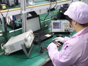
Step 7: Electrical Testing
- Objective: Verify the electrical integrity of the manufactured PCB.
- Process:
- Each PCB undergoes electrical testing to check for short circuits, open circuits, and other faults using automated test equipment. This ensures all the intended connections are correctly established.
Step 8: Cutting and Profiling
- Objective: Separate individual PCBs from larger panels and shape them according to design specifications.
- Process:
- A router or v-cut machine is used for precise cutting and profiling the PCBs into the desired form factors. The edges are smoothed to remove any burrs or sharp points.
The manufacturing process of PCBs is a blend of art and science, requiring precision timing and control at every stage to produce reliable and high-quality circuit boards. Each step builds upon the last to ensure the final product meets both design and industry specifications, ready for the next phase of electronic assembly.
Chapter 6
PCB Assembly Techniques
PCB assembly is the process of mounting and soldering electronic components onto a printed circuit board. The choice of assembly technique depends on various factors like the type of components used, the complexity of the circuit, and the intended application of the PCB. Two primary assembly techniques are Surface-Mount Technology (SMT) and Through-Hole Technology (THT). Here’s an exploration of these techniques:
Surface-Mount Technology (SMT)
Definition: SMT involves directly mounting electronic components onto the surface of the PCB. Components used in this process are known as Surface-Mount Devices (SMDs).
Process:
- Solder Paste Application: A stencil is used to apply a viscous solder paste onto the pad areas of the PCB where components will be placed.
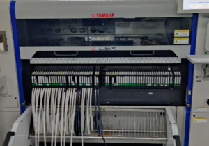
- Pick and Place: Automated machines pick components from reels or trays and accurately place them onto the board at designated locations.
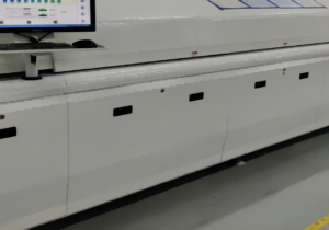
- Reflow Soldering: The assembled board passes through a reflow oven where the solder paste melts and solidifies, creating robust electrical and mechanical connections.
Advantages:
- Miniaturization: Supports smaller and lighter components, allowing for more compact, high-density designs.
- Automation: Highly amenable to automation, reducing labor costs and increasing production rates.
- Performance: Offers better performance for high-frequency applications due to reduced lead inductance and parasitic capacitance.
Applications: Widely used in consumer electronics, telecommunications, automotive electronics, and more, where high component density and miniaturization are desired.
Through-Hole Technology (THT)
Definition: THT involves inserting component leads through pre-drilled holes in the PCB and soldering them on the opposite side. These components are often larger with leads designed to go through the board.
Process:
- Component Insertion: Components are manually or automatically inserted into the PCB with leads extending through the holes.
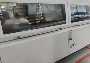
- Soldering: Typically, wave soldering is used for mass production. The PCB passes over a wave of molten solder that adheres to exposed metal areas, sealing the components in place.
Advantages:
- Mechanical Strength: Provides strong mechanical bonds, making it suitable for components that will undergo mechanical stress.
- Prototyping and Testing: Easier to handle and modify, making it ideal for prototyping and test applications.
- Applications: Preferred in applications requiring high reliability and durability, such as industrial machinery, military equipment, and aerospace, where the mechanical strength of the solder joints is crucial.
Combining SMT and THT
- Mixed Technology Boards: Many modern PCBs use a combination of SMT and THT, leveraging the benefits of both methods.
- Application Strategy: Critical or high-power components are often mounted through-hole for added strength, while passive components, ICs, and other small devices are surface-mounted to save space and take advantage of automated assembly processes.
Additional Assembly Considerations
- Component Orientation: Accurate orientation and alignment are crucial to avoid assembly errors and ensure functional operation.
- Thermal Management: Adequate heat dissipation techniques need to be considered, especially in high-density SMT designs, to prevent overheating and maintain performance.
- Inspection and Quality Control: Post-assembly, boards undergo thorough inspection, either manually or using automated optical inspection (AOI) systems, to ensure high-quality solder joints and proper placement of all components.
PCB assembly techniques are integral to the production of effective and reliable electronic devices. By understanding and selecting the appropriate assembly method based on application needs and component types, manufacturers can optimize the performance and cost-effectiveness of electronic products.
Chapter 7

Quality Assurance in PCB Fabrication
Quality assurance (QA) is a critical component of PCB fabrication, ensuring that each board produced meets the required standards for reliability, performance, and safety. It involves a systematic approach to evaluate and improve the design, manufacturing processes, and final product quality. Here’s an in-depth look at the quality control measures and testing methodologies used in PCB fabrication:
1. Design Verification
- Objective: Ensure the PCB design meets specification and manufacturability guidelines before production.
- Tools and Processes:
- Design Rule Check (DRC): Automated checks within EDA tools to verify that the design adheres to the defined manufacturing constraints and design specifications.
- Electrical Rule Check (ERC): Checks the schematic for connectivity issues and potential electrical errors.
2. Incoming Material Inspection
- Purpose: Verify the quality of raw materials (laminates, copper foil, prepreg, components) before they enter production.
- Inspection Criteria:
- Visual inspection for any defects or contamination.
- Measurement of thickness, surface smoothness, and adherence properties.
- Electrical tests for dielectric properties and conductivity.
3. In-Process Quality Control
- Objective: Monitor the manufacturing process to detect defects early and minimize waste.
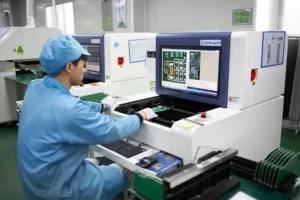
- Techniques:
- Automated Optical Inspection (AOI): High-resolution cameras inspect each layer after important processes (e.g., etching, solder mask application) to ensure pattern fidelity and alignment.
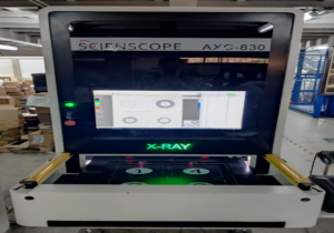
- X-ray Inspection: Used to inspect inner layers, vias, and solder joints, particularly in SMT assemblies where visual inspection is not feasible.
- Statistical Process Control (SPC): Uses statistical methods to monitor and control the manufacturing process for consistent quality output.
4. Electrical Testing
- Objective: Confirm that each PCB functions as intended without electrical faults.
- Testing Methods:
- In-Circuit Testing (ICT): Checks the functionality of individual components and their connections on the assembled board.
- Flying Probe Test: A non-contact test that uses probes to test electrical connections and component values, particularly for prototypes or smaller batches.
- Functional Testing: Tests the assembled PCB in a setup that mimics its final operational environment to ensure proper operation.
5. Environmental and Stress Testing
- Purpose: Assess the PCB’s durability and performance under various environmental conditions.
- Testing Scenarios:
- Thermal Cycling: Expose the PCB to extreme temperature variations to test thermal stability and solder joint integrity.
- Humidity and Moisture Testing: Evaluates the board’s resistance to moisture, which can lead to corrosion or short circuits.
- Vibration and Shock Testing: Simulates mechanical stresses the PCB may encounter during shipping or in its working environment.
6. Final Inspection and Review
- Objective: Ensure the finished PCBs adhere to customer specifications and industry standards before delivery.
- Processes:
- Visual Inspection: Verify labeling, silkscreen legibility, and overall board aesthetics.
- Dimensional Checks: Ensure physical dimensions are within specified tolerances.
- Review of Test Results: Analyze all data collected throughout the QA process to certify product quality and identify areas for process improvement.
7. Documentation and Traceability
- Purpose: Maintain comprehensive records for accountability and continuous improvement.
- Documentation:
- Detailed records of every inspection, test results, and corrective actions taken.
- Labeling and coding each PCB for traceability to identify issues back to specific batches or processes.
Effective quality assurance in PCB fabrication is instrumental in delivering high-quality, reliable products. By implementing robust QA processes and embracing technological advancements in testing and inspection, manufacturers can enhance product reliability, reduce defects, and ensure customer satisfaction.
Chapter 8
Choosing the Right PCB Fabrication Partner
Selecting the right PCB fabrication partner is crucial for ensuring the quality, reliability, and timely delivery of your printed circuit boards. A good partner can help you navigate the complexities of the manufacturing process, provide valuable insights, and ultimately contribute to the success of your projects. Here are some tips and criteria to consider when selecting a PCB manufacturer:
1. Evaluate Technical Capabilities
Manufacturing Technology: Ensure the manufacturer has the technology to meet your specific requirements, whether it’s for standard, high-density, multilayer, flexible, or rigid-flex PCBs.
- Advanced Processes: Look for capabilities such as laser drilling, via plugging, blind/buried vias, and HDI technology if your design demands these features.
- Volume Flexibility: Check if the manufacturer can handle your required production volume—be it prototype, medium, or mass production.
2. Assess Quality Certifications
- ISO Certification: Confirm the manufacturer is ISO 9001 certified, indicating a commitment to quality management systems and consistent process improvements.
- IPC Standards: Ensure adherence to IPC standards, which govern the quality and reliability of electronics assemblies.
- UL Certification: Check if products meet UL (Underwriters Laboratories) safety standards, particularly if your boards are destined for markets with stringent safety regulations.
3. Experience and Reputation
- Track Record: Look for manufacturers with a proven history in the industry, especially with projects similar to yours.
- Clientele: Research the manufacturer’s clientele to gauge their market presence and expertise in different sectors (e.g., automotive, telecommunications, consumer electronics).
4. Product Quality and Testing
- Quality Assurance Processes: Inquire about their quality assurance procedures, in-process testing capabilities, and final inspection routines.
- Certifications: Request information on any additional quality or reliability testing certifications they might offer, like RoHS compliance for environmental standards.
5. Customer Service and Communication
- Responsiveness: Evaluate how quickly and efficiently the manufacturer responds to inquiries and how communicative they are throughout the process.
- Technical Support: A good partner offers robust technical support to assist with design queries, production challenges, and post-production troubleshooting.
6. Pricing and Cost Transparency
- Competitive Pricing: Request detailed quotations and compare them across several manufacturers to ensure pricing is competitive without compromising quality.
- Cost Breakdown: Ensure transparency in pricing, with clear breakdowns of costs, including setup, material, labor, and any additional charges.
7. Turnaround Time and Delivery Reliability
- Lead Times: Confirm their standard lead times and assess their capacity for expedited services when quicker delivery is critical.
- Supply Chain Efficiency: Assess their supply chain robustness to gauge how well they can handle disruptions and maintain reliable delivery times.
8. References and Reviews
- Customer Reviews: Look for reviews or testimonials from previous clients to gain insight into the manufacturer’s reliability, service quality, and customer satisfaction.
- Reference Checks: Don’t hesitate to ask for references and directly contact past clients to discuss their experiences with the manufacturer.
9. Innovation and R&D
- Adaptability: Partner with a manufacturer who keeps abreast of the latest industry innovations and advancements, ensuring your designs benefit from cutting-edge technology.
- Collaborative Engagement: Find a partner who engages collaboratively, offering suggestions for design improvements and cost optimizations.
Choosing the right PCB fabrication partner requires careful consideration of numerous factors beyond just cost. By evaluating their capabilities, certifications, experience, and customer service, you can form a strategic partnership that leads to successful, high-quality PCB production tailored to your specific needs.
Chapter 9
Common Challenges and Solutions in PCB Assembly
PCB assembly is a complex process that can present several challenges, impacting the efficiency, cost, and reliability of electronic products. Identifying these challenges early and implementing practical solutions is essential for maintaining smooth and successful assembly operations. Here’s a detailed look at some common challenges and strategies to overcome them:
1. Solder Joint Defects
- Challenges: Solder joint defects, such as insufficient solder, cold solder joints, and bridging, can lead to electrical failures and decreased product reliability.
- Solutions:
- Solder Paste Inspection (SPI): Implement pre- and post-reflow inspections using SPI systems to ensure proper paste deposition.
- Optimal Reflow Profiles: Fine-tune the reflow oven profile to ensure optimal heating and cooling rates, preventing defects like cold solder joints.
- Design for Manufacturability (DFM): Collaborate with design engineers to optimize pad sizes and stencils, reducing the likelihood of bridging.
2. Component Placement Issues
- Challenges: Misaligned, missing, or incorrectly oriented components can cause functional failures and rework.
- Solutions:
- Precision Pick-and-Place Machines: Use high-accuracy pick-and-place machines equipped with vision systems to ensure precise component placement.
- Component Verification: Implement automated optical inspection (AOI) to verify component placement and orientation before soldering.
3. Thermal Management
- Challenges: Improper thermal management can lead to overheating, affecting solder joint integrity and component performance.
- Solutions:
- Thermal Profiling: Develop accurate thermal profiles tailored to the unique thermal mass of each assembly.
- Heat Dissipation Design: Incorporate thermal vias, heat sinks, and adequate clearance in board design to enhance heat dissipation.
4. Handling of Fine-Pitch and Miniaturized Components
- Challenges: As components shrink in size, the difficulty of handling and accurately placing them increases.
- Solutions:
- Advanced Equipment: Use state-of-the-art assembly equipment capable of handling fine-pitch and ultra-small components with precision.
- Skilled Workforce: Invest in training for workers to handle and inspect small components effectively.
5. Electromagnetic Interference (EMI)
- Challenges: EMI can cause signal degradation and functional disruptions in sensitive electronic assemblies.
- Solutions:
- Shielding and Grounding: Design PCBs with proper grounding and electromagnetic shielding.
- Component Layout: Optimize component layout to minimize EMI emissions and susceptibility.
6. Moisture Sensitivity
- Challenges: Moisture absorption by components can lead to solder defects such as popcorning during reflow.
- Solutions:
- Controlled Storage: Store moisture-sensitive components in desiccant conditions with proper moisture barrier bags and humidity indicators.
- Bake Out Procedures: Implement bake out procedures to remove absorbed moisture from components prior to assembly.
7. Testing and Inspection Complexity
- Challenges: As assemblies become more complex, thorough testing is essential yet challenging.
- Solutions:
- Automated Testing: Implement flying probe testers and in-circuit testing (ICT) to automate the testing of complex configurations.
- Functional Testing: Set up tests that mimic real-world usage to verify full operational capability of the PCB assembly.
8. Supply Chain Disruptions
- Challenges: Component lead times and availability fluctuations can delay assembly processes.
- Solutions:
- Vendor Relationships: Strengthen vendor relationships and diversify supply sources to minimize dependence on a single supplier.
- Inventory Management: Implement robust forecasting and inventory management practices to anticipate and mitigate component shortages.
By understanding these common challenges in PCB assembly and applying targeted solutions, manufacturers can enhance product quality, reduce production times, and minimize costs. Continuous improvement in assembly processes, equipment, and training is key to overcoming these hurdles and achieving reliable and efficient PCB assembly.
Chapter 10
Future Trends in PCB Technology
The PCB industry is continually evolving, driven by the demand for more powerful, efficient, and compact electronic devices. Emerging trends in PCB fabrication and assembly reflect advancements in materials, miniaturization, and integration technologies. Here’s an overview of some key future trends shaping the industry:
1. Advanced Materials
- High-Performance Substrates: The development of advanced substrate materials, such as liquid crystal polymers (LCP) and polyimide, is enabling better thermal management, higher frequency performance, and flexibility in PCB designs.
- Environmentally Friendly Materials: With increased environmental concerns, there is a shift towards using eco-friendly materials that comply with RoHS and other environmental standards.
2. Miniaturization and High-Density Interconnection (HDI)
- Increased Component Density: Advances in HDI technology are allowing for more components to be packed into smaller areas, enhancing functionality without increasing board size.
- Microvias and Via-in-Pad Designs: These techniques are being used to further reduce PCB size while maintaining or increasing performance levels.
3. Flexible and Rigid-Flex PCBs
- Adaptability and Versatility: Flexible and rigid-flex PCBs are gaining traction, especially in industries like wearables, medical devices, and automotive, where space constraints and flexible design are key.
- Bendable Electronic Solutions: These PCBs enable innovative designs that can bend, fold, and flex, opening new possibilities for product design and function.
4. Integration of 3D Printing
- Additive Manufacturing: The use of 3D printing in PCB fabrication is becoming more prevalent, enabling rapid prototyping, complex geometries, and potentially lower costs for small production runs.
- Embedded Components: 3D printing can facilitate the embedding of components directly within the PCB structure, further reducing size and improving reliability.
5. Internet of Things (IoT) Integration
- IoT-Ready Designs: With the proliferation of IoT devices, PCBs are increasingly designed to support wireless communication modules and IoT functionalities, driving the need for compact, multifunctional designs.
- Energy Efficiency: IoT applications push the development of energy-efficient PCBs that can operate with minimal power consumption.
6. Enhanced Automation and AI
- Smarter Manufacturing: The integration of AI and machine learning into PCB manufacturing processes is enhancing predictive maintenance, optimizing workflows, and reducing errors.
- Automated Quality Control: Advanced vision systems and AI-driven inspection technologies are leading to faster, more accurate quality control processes.
7. Thermal Management Solutions
- Integrated Heat Dissipation: As electronic devices become more powerful, the need for integrated thermal management solutions within the PCB itself is crucial to maintain performance and reliability.
- Innovative Materials: The use of materials like graphene and other composites is being explored to improve heat conduction across PCBs.
8. Advanced Signal Integrity
- High-Speed Data Transmission: As demand for high-speed data processing grows, PCBs are being designed with improved signal integrity to support faster communication without signal loss.
- EMI Shielding: Enhanced EMI shielding solutions are becoming integral in PCB design to prevent interference in critical applications such as automotive and aerospace electronics.
These future trends in PCB technology highlight the industry’s response to evolving demands for more sophisticated, efficient, and compact electronic solutions. As technology progresses, PCB design and manufacturing will continue to innovate, meeting the requirements of next-generation electronic devices with advanced and adaptable solutions.
Get in touch
Where Are We?
Industrial Park, No. 438 Donghuan Road, No. 438, Shajing Donghuan Road, Bao'an District, Shenzhen, Guangdong, China
Floor 4, Zhihui Creative Building, No.2005 Xihuan Road, Shajing, Baoan District, Shenzhen, China
ROOM A1-13,FLOOR 3,YEE LIM INDUSTRIAL CENTRE 2-28 KWAI LOK STREET, KWAI CHUNG HK
service@southelectronicpcb.com
Phone : +86 400 878 3488
Send us a message
The more detailed you fill out, the faster we can move to the next step.

