
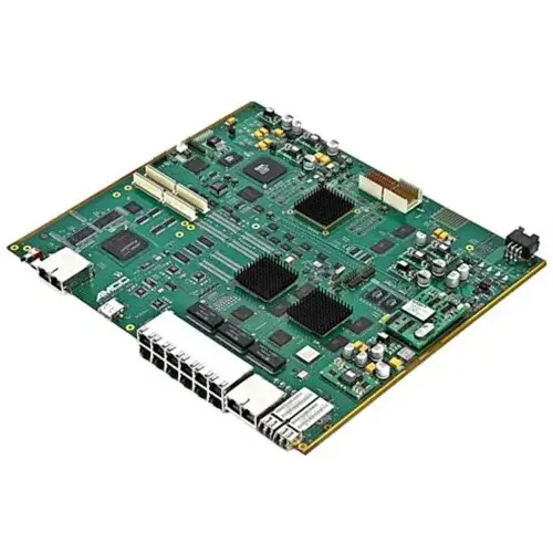
PCB Prototyping
South-Electronic
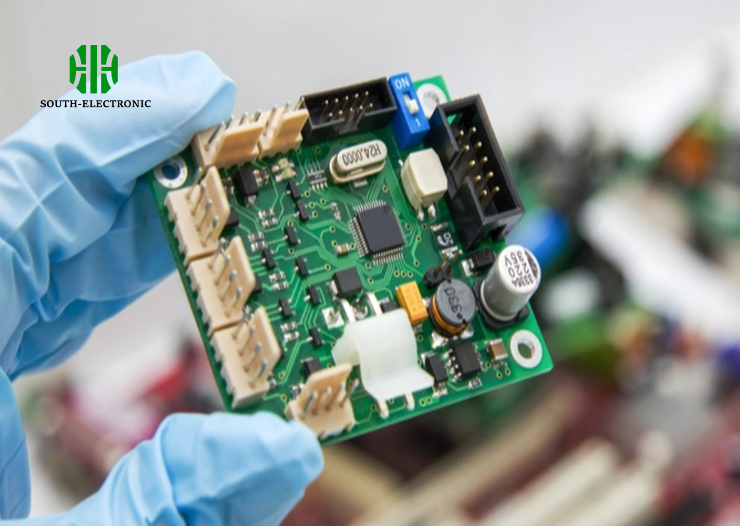
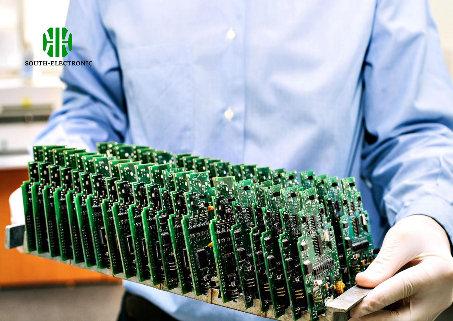
Choose South-Electronic for unbeatable quality, reliability, and incredible value in your prototyping needs. Experience the difference with our all-in-one PCB prototyping service – from idea to finished product, we guarantee precision, speed, and adherence to your unique specifications.
Your Trusted Provider of PCB Prototyping
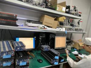
Welcome to South-Electronic, where you’ll find high-quality PCB prototyping services renowned for their precision and rapid turnaround.
Our prototyping ensures superior performance, making it ideal for testing a diverse range of applications before full-scale production. Explore various configurations like single-layer, double-layer, and multi-layer prototypes, all tailored to accelerate your development process.
Why Choose South-Electronic?
-
Flexibility in Ordering
Order exactly what you need, when you need it.
Whether you're looking for a single prototype or multiple iterations, we tailor every order to meet your unique requirements, ensuring a flexible and smooth process for you. -
Experienced Team
Tap into industry expertise for your next project.
With over a decade of experience, our team is here to help you achieve success with the insights and knowledge we've gained from working across the industry. -
Guartneed Quality
Enjoy the best quality, straight from the manufacturer.
As your primary manufacturer, we guarantee top-notch quality that exceeds what you'll find from other suppliers, giving you the peace of mind you deserve. -
Fast Delivery
Get your orders fast with our efficient production processes.
We understand that time matters. Our streamlined operations ensure you receive your products quickly, keeping your projects on track without delay. -
Guaranteed Satisfaction
All-in-one PCB solutions designed for your satisfaction.
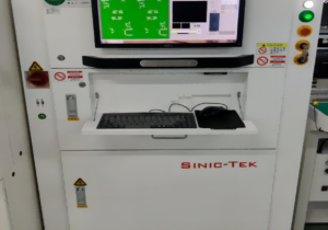
With our extensive range of processing equipment, we provide comprehensive services to meet all your PCB needs, ensuring a seamless experience from start to finish.
Related Project We had Done
Customer Reviews
engineer
thank you, guys, the boards are really good, i am really happy to receive my boards, the components are perfect!

Operation Manager
South-Electronic is my first PCBA supplier in China. The service and quality are excellent, and the after-sales support is also very impressive. Good Job!


Common Questions
Most Popular Questions
Usually 2- 3 week. fastest 3 days.
Absolutely, we offer PCB design help as part of our prototyping services. Our team of experts will work closely with you to understand your specific needs and project objectives.
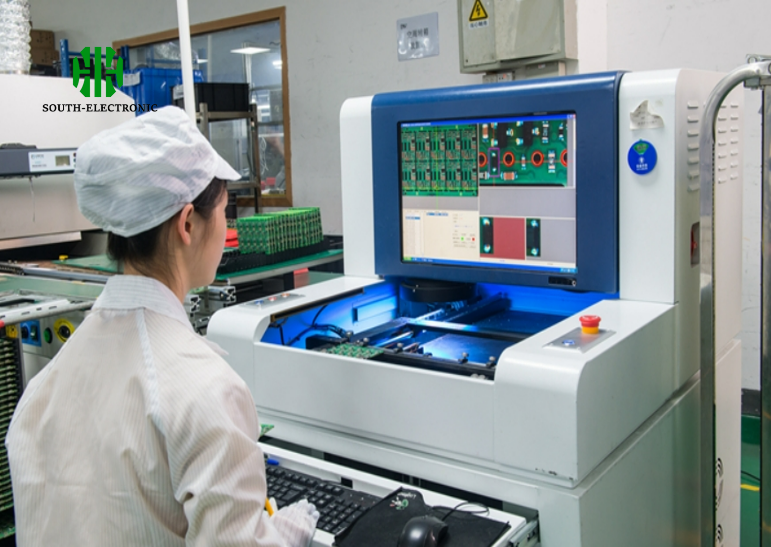
Every PCB prototype undergoes rigorous testing and quality checks to ensure compliance with our high standards. As an ISO9001 certified facility, we are committed to delivering prototypes that meet or exceed customer expectations. Our quality assurance measures include electrical testing, visual inspection, and material verification.
South-Electronic accepts bank transfers, major credit cards, and online payments through platforms like Alibaba.
Send us a message
The more detailed you fill out, the faster we can move to the next step.


The Complete Guide For PCB Prototyping
Contents
Chapter 1
Introduction to PCB Prototyping
PCB prototyping is a crucial step in the development of electronic devices. It allows designers and engineers to test their circuit designs in a real-world scenario before committing to large-scale production. The goal of PCB prototyping is to create a functional, small-scale version of the final product, which helps identify any design flaws, electrical issues, or mechanical constraints early on. By catching potential problems at this stage, companies can save time and money while ensuring the final product performs as expected.
What is PCB Prototyping?
PCB prototyping involves designing and producing a limited number of physical circuit boards to validate the functionality of a design. It helps bridge the gap between the concept and mass production stages. Prototyping provides the opportunity to test how well components interact, assess the integrity of signal pathways, and troubleshoot potential performance issues, all in a controlled, small-scale environment. It is an iterative process, often requiring several versions of the prototype before arriving at a final design that’s ready for production.
Why is PCB Prototyping Important?
PCB prototyping is important for several reasons:
Risk Mitigation: Early detection of design flaws reduces the risk of costly mistakes in the production phase.
Testing and Validation: Prototyping ensures that the circuit functions as intended under real-world conditions, validating both electrical performance and mechanical structure.
Design Optimization: Prototypes allow engineers to experiment with component placement, routing strategies, and other design elements to optimize performance and cost.
Shortened Time to Market: By resolving issues early in the design process, the overall timeline for bringing a product to market is shortened, making the development process more efficient.
Chapter 2
Design Considerations
Designing a printed circuit board (PCB) prototype involves many crucial decisions that impact the performance, reliability, and manufacturability of the final product. Getting the design right in the early stages of prototyping is essential for ensuring that the board works as intended and avoids costly reworks later. In this section, we’ll cover key PCB design considerations that must be taken into account during the prototyping phase, including component placement, trace routing, signal integrity, power management, and manufacturability.
1. Component Placement
One of the first and most critical steps in PCB design is determining the optimal placement of components. Proper component placement can enhance performance, simplify trace routing, and ensure that the board is easy to assemble and maintain. Here are key guidelines to follow:
- Group Related Components Together: Components that work together should be placed close to each other to reduce trace lengths and minimize potential signal delays. For instance, decoupling capacitors should be placed near the power pins of ICs to filter noise efficiently.
- Place Sensitive Components Strategically: Analog components, high-frequency circuits, and sensitive components such as oscillators should be placed away from noisy digital circuits to prevent interference.
- Consider Heat Management: Power components that generate heat, such as regulators or power transistors, should be spaced out to avoid overheating. Ensure there’s room for heat sinks or thermal vias to manage heat dissipation effectively.
- Component Orientation: For ease of assembly, components should be oriented consistently, especially if using automated pick-and-place machines. This reduces the chance of errors during the assembly process.
2. Trace Routing
Trace routing is critical to ensuring signal integrity and reliable electrical connections on the PCB. Poor routing can lead to signal degradation, noise, and even complete failure of the circuit.
- Key considerations include:Minimize Trace Lengths: Shorter traces reduce resistance and inductance, helping to maintain signal quality. For high-frequency or high-speed signals, longer traces can cause signal delays or reflections, so keep them as short as possible.
- Follow the 90/45-Degree Rule: Avoid sharp 90-degree angles when routing traces, as these can cause signal reflection and EMI (electromagnetic interference). Instead, use 45-degree bends to improve signal flow.
- Use Wide Traces for Power Lines: Power traces, especially those carrying higher currents, should be wider than signal traces to reduce voltage drops and prevent overheating. You can use online trace width calculators to determine the correct width based on current levels.
- Controlled Impedance: For high-speed or RF designs, maintaining controlled impedance along traces is essential. This often requires careful consideration of trace width, spacing, and the dielectric material used in the PCB.
3. Ground Planes and Power Distribution
Proper grounding and power distribution are essential to avoid noise, voltage fluctuations, and signal degradation in the PCB design. Some considerations include:
- Dedicated Ground Plane: A continuous ground plane in a multi-layer PCB provides a low-impedance path for return currents and reduces EMI. It also helps to improve signal integrity and reduces the chance of noise coupling.
- Power Plane: A separate power plane is recommended to deliver a stable voltage supply to all components. This reduces the resistance and inductance associated with traditional power traces and helps maintain consistent voltage levels.
- Decoupling Capacitors: Use decoupling capacitors to filter out noise from the power supply. These should be placed as close as possible to the power pins of integrated circuits to be most effective.
- Star Grounding: For sensitive analog circuits, consider a star grounding configuration to avoid ground loops, where each sub-circuit has its own path to the main ground, preventing interference between circuits.
4. Signal Integrity and EMI Management
Signal integrity refers to the quality and accuracy of the electrical signals traveling through the PCB. Managing electromagnetic interference (EMI) is also vital to avoid signal degradation. Important design considerations include:
- Keep High-Speed Signals Separate: High-speed signals can cause significant EMI and cross-talk. To reduce interference, keep these signals away from other sensitive signals by using isolation techniques such as shielding or distance separation.
- Differential Pair Routing: For high-speed signals like USB or HDMI, use differential pair routing, where two complementary signals are routed together to cancel out noise. Ensure that these traces are of equal length to prevent signal skewing.
- Signal Termination: Use appropriate termination resistors to match impedance for high-speed signal lines. This prevents signal reflection and maintains signal integrity over longer traces.
- Grounding Via Placement: Use stitching vias to connect ground planes across multiple layers. This helps reduce high-frequency noise and ensures a stable ground reference throughout the PCB.
5. Thermal Management
Effective thermal management is essential, especially for PCBs with power components or high current. Overheating can lead to component failure or degraded performance over time. Key considerations include:
- Thermal Vias: For components that generate significant heat, use thermal vias to transfer heat away from the component into other areas of the board or to a heat sink.
- Heat Sinks and Thermal Pads: Components such as voltage regulators or power transistors may require heat sinks or thermal pads to dissipate heat efficiently. Ensure there’s enough space on the board to accommodate these features.
- Component Spacing: Proper spacing between components can improve airflow, especially in designs where forced air cooling is used. Overcrowding components can trap heat and cause localized hot spots.
Conclusion
When designing a PCB prototype, careful consideration of component placement, trace routing, grounding, power management, signal integrity, and manufacturability is essential. Each of these factors plays a critical role in ensuring that the PCB operates efficiently, meets performance expectations, and can be produced at a reasonable cost. By addressing these design considerations early in the prototyping process, you can create a PCB that is not only functional but also scalable for mass production, helping you achieve a faster time to market and a more reliable end product.
Chapter 3

PCB Layout Tips
Making a good PCB layout is crucial for a successful prototype. It guarantees reliable functionality, manufacturability, and performance. Here are some important tips for optimizing your PCB layout during the prototyping phase:
Optimize Component Placement
Trace Routing
- Short, Direct Traces: Keep traces short to reduce resistance and improve signal integrity.
- Avoid 90-Degree Angles: Use 45-degree angles to reduce EMI and signal reflection.
- Correct Trace Width: Ensure power traces are wide enough to handle current without overheating.
Ground and Power Planes
- Dedicated Ground Plane: Use a full-layer ground plane to minimize noise and improve signal integrity.
- Power Plane: Ensure a stable power supply by using a dedicated power plane, which reduces parasitic inductance and resistance.
Signal Integrity
- High-Speed Signals: Route high-speed signals first and use differential pair routing where necessary. Keep these traces short and away from noise sources.
- Impedance Control: For high-frequency designs, ensure traces maintain controlled impedance to avoid signal loss.
Thermal Management
- Thermal Vias: Use thermal vias to dissipate heat from power components.
- Copper Pours: Include large copper areas to help with heat dissipation and stabilize the temperature.
Design for Manufacturability
- Standard Components: Use commonly available component sizes to reduce costs and simplify assembly.
- Sufficient Clearance: Ensure ample spacing between traces and components to avoid shorts or assembly issues.
- Test Points: Include test points for easy troubleshooting during the prototyping phase.
Mechanical Constraints
- Board Shape and Size: Ensure the PCB fits within its enclosure, with room for connectors and mounting holes.
- Connector Placement: Align connectors on the edge for easy access, ensuring proper clearance for external connections.
Conclusion
Following these PCB layout tips during prototyping helps ensure a reliable, functional, and manufacturable design. Proper planning, efficient routing, and careful consideration of power, thermal, and mechanical factors are key to a successful PCB layout.
Chapter 4
Material Selection
Choosing the right materials for your PCB (Printed Circuit Board) prototype is critical to ensuring optimal performance, durability, and manufacturability. The materials you choose will determine the electrical, thermal, and mechanical properties of the board, which directly affect the functionality and reliability of the final product. Different applications require specific material properties based on factors such as the operating environment, signal speed, and component density.
Substrate Material
The substrate material is the foundation of a PCB. It provides the physical structure and supports the copper traces that carry signals. The most common types of substrate materials are FR4, polyimide, and Rogers materials, each suited for different applications based on their electrical and thermal characteristics.
- FR4 (Flame Retardant 4): FR4 is the most widely used substrate material for PCBs, offering a good balance of cost, durability, and performance. Made of woven fiberglass reinforced with epoxy resin, it has excellent mechanical strength and good electrical insulation. FR4 is suitable for general-purpose PCBs, handling moderate signal speeds and frequencies. It is a versatile material that works well in various applications, including consumer electronics, industrial devices, and automotive systems.
- Polyimide: Polyimide is used in flexible or rigid-flex PCBs, especially where the board needs to be folded or bent, such as in wearable devices, medical implants, or aerospace applications. Polyimide is known for its excellent thermal stability, capable of withstanding extreme temperatures, making it ideal for harsh environments.
- Rogers Material: Rogers is a family of high-performance laminates used in applications that require high-frequency signal transmission, such as RF (Radio Frequency) and microwave circuits. Rogers materials offer low dielectric loss and stable dielectric properties, making them ideal for high-speed or high-frequency applications like 5G, aerospace, and advanced radar systems.
Key Considerations for Substrate Material Selection
- Signal Speed and Frequency: Low dielectric constant materials like Rogers are preferred for high-speed or high-frequency circuits.
- Thermal Environment: If the PCB will be exposed to high temperatures, consider polyimide or other high-temperature-resistant materials.
- Mechanical Flexibility: Polyimide is the go-to material for flexible PCBs. FR4 is generally sufficient for rigid boards.
- Cost vs. Performance: FR4 is cost-effective and suitable for general-purpose use. However, for specialized applications that require high-frequency performance, higher-cost materials like Rogers may be necessary.
Copper Thickness
The copper layer on a PCB is critical for conducting electricity, and its thickness determines the board’s current-carrying capacity and thermal dissipation properties. Copper thickness is typically measured in ounces per square foot (oz/ft²) or in microns.
- Standard Copper Thickness: For most PCB designs, the standard copper thickness is 1 oz/ft², which is equivalent to approximately 35 microns. This is sufficient for most low-power, signal transmission, and control circuit designs.
- Heavy Copper: In high-power applications, such as power supplies or motor controllers, heavy copper PCBs (2 oz/ft² or more) are used to handle higher current loads and dissipate more heat. Heavy copper traces are also more robust and durable, offering a longer service life in harsh conditions.
- Thin Copper: For high-density, fine-pitch designs, thin copper layers (e.g., 0.5 oz/ft² or 17.5 microns) are often used. Thin copper is more suitable for high-speed signal circuits, where reducing trace thickness helps maintain signal integrity and minimize parasitic capacitance and inductance.
Key Considerations for Copper Thickness:
- Current-Carrying Requirements: Thicker copper is needed for higher currents to prevent overheating or excessive voltage drops.
- Thermal Dissipation: Thicker copper layers help dissipate heat more effectively for power circuits.
- Signal Integrity: Thinner copper can reduce signal distortion in high-speed circuits, but it may be less durable in power circuits.
Dielectric Properties
Dielectric materials in PCBs play a crucial role in insulating copper layers and maintaining signal integrity, especially in high-frequency designs. Important dielectric properties include the dielectric constant (Dk) and dissipation factor (Df).
Dielectric Constant (Dk): The dielectric constant measures a material’s ability to store electrical energy. Lower Dk materials allow signals to travel faster through the PCB. FR4 has a dielectric constant of about 4.5, while materials like Rogers may have a Dk as low as 2.2, making them suitable for high-speed signal transmission.
Dissipation Factor (Df): Df represents how much signal energy is lost as heat. A lower dissipation factor is crucial for maintaining signal integrity in high-frequency circuits, as it minimizes energy loss during signal transmission. Rogers materials typically have a lower Df compared to FR4, making them better for high-frequency and RF applications.
conclusion
It is important to carefully consider the materials used in your PCB prototype in order to meet the electrical, thermal, and mechanical requirements of the board. Whether it is choosing the right substrate, such as FR4 for general purposes or Rogers for high-frequency applications, or selecting the appropriate copper thickness, dielectric properties, and surface finishes, each decision will impact the final performance and cost of the PCB.
Chapter 5
Prototyping Tools and Techniques
When it comes to PCB prototyping, the right tools and techniques can make all the difference. In this guide, we’ll take a look at some of the essential tools and techniques used in PCB prototyping, including design software, fabrication methods, assembly equipment, and testing tools.
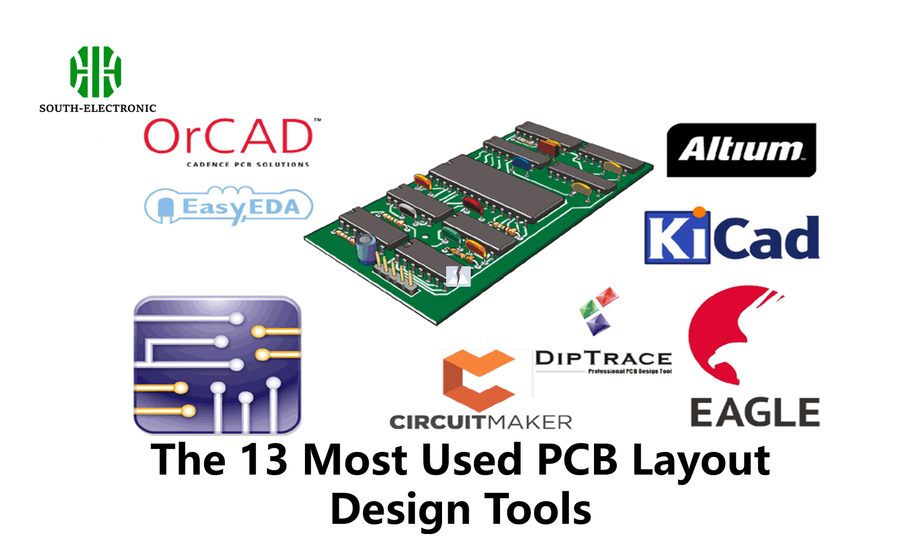
PCB Design Software
The first step in PCB prototyping is designing the board layout using specialized CAD (Computer-Aided Design) software. These tools allow engineers to create a detailed schematic of the circuit, define component placement, and plan the routing of electrical connections. Some popular PCB design software includes:
- Altium Designer: A comprehensive, professional-grade tool that is widely used for complex PCB designs. It offers advanced features for multi-layer boards, signal integrity analysis, and 3D visualization, making it suitable for high-performance designs.
- Eagle: A widely used, user-friendly tool that is great for smaller projects. It includes schematic capture, PCB layout, and autorouting capabilities. Eagle is favored by hobbyists and small businesses due to its affordability and ease of use.
- KiCad: An open-source PCB design tool with a strong community of users. It’s free and offers many of the features found in commercial software, such as multi-layer PCB support, footprint libraries, and schematic editing.
- OrCAD: A robust solution for larger, more complex designs, offering simulation tools and powerful design rule checks. It is often used for industrial and professional projects where precision and scalability are key.
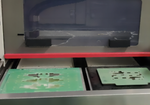
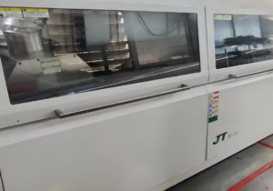
PCB Fabrication Techniques
Once the design is finalized, the next step is fabricating the PCB prototype. Several fabrication techniques can be used, depending on the complexity of the board and the available resources. The most common methods include:
- CNC Milling: CNC (Computer Numerical Control) milling is a subtractive process where material is removed from a copper-clad board using a milling machine. CNC milling is well-suited for low-cost, quick-turn prototypes and small production runs. It is widely used for single-layer or simple double-layer PCBs.
- Laser Etching: Laser etching uses a high-precision laser to remove copper from the board, creating the traces. This method is highly accurate and allows for fine-pitch designs. However, it requires specialized equipment and is typically used for high-performance, high-frequency circuits.
- Photoresist and Etching: In this technique, a photoresist film is applied to the copper-clad board. The board is then exposed to UV light through a mask, and the unexposed areas are etched away using chemicals. This method is suitable for more complex, multi-layer PCBs and can achieve high trace density.
- 3D Printing: Emerging as a viable option for PCB prototyping, 3D printing allows the rapid creation of boards by printing conductive materials directly onto a substrate. While not as widely used for traditional PCBs, this technique is useful for prototyping flexible PCBs or non-standard designs.
Choosing a Fabrication Technique:
When choosing a fabrication technique, consider factors such as cost, complexity, and turnaround time. CNC milling is ideal for quick, simple prototypes, while photoresist etching is better for complex, multi-layer boards. Laser etching provides high precision for fine-pitch designs. 3D printing is a flexible option for specialized projects.
Conclusion
The success of PCB prototyping depends largely on using the right tools and techniques for each stage of the process. From the initial design in CAD software to fabrication methods like CNC milling and assembly techniques such as SMT, every step requires precision and attention to detail. Additionally, testing and debugging tools ensure the prototype functions as intended before moving into production. By selecting the appropriate tools and techniques, you can streamline the prototyping process and create a reliable, high-quality PCB.
Chapter 6
Manufacturing the Prototype
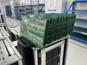
Once you have your PCB design finalized and you’ve used prototyping tools and techniques to develop a working design, the next step is to manufacture the prototype. PCB manufacturing involves taking the digital design and turning it into a physical board through a series of precise and technical processes. This includes several key steps such as material preparation, layer stacking, drilling, plating, and quality inspection. Understanding the manufacturing process is important to ensure that your prototype is produced accurately and performs as intended.
Preparing Materials and Design Files
Before you start manufacturing, you need to prepare your design files and send them to the manufacturer. These files, typically in Gerber format, contain all the information needed to produce the PCB, including the copper layer layout, drill patterns, solder mask, and silkscreen. It’s important to prepare these files properly to avoid errors during production.
- Gerber Files: These are industry-standard files that show the exact layout of each layer of your PCB. You’ll have separate Gerber files for your copper layers, solder masks, silkscreen, and drill patterns. Make sure these files are generated correctly and verified before you send them to the manufacturer.
- Bill of Materials (BOM): The BOM lists all the components you need for your PCB, including their specifications, part numbers, and where they go on the board. This document is important to make sure you order the right components and use them during the assembly process.
- Design Rule Check (DRC): Before you start manufacturing, run a DRC in your design software to make sure your board adheres to the manufacturer’s capabilities, such as minimum trace width, spacing, and hole size. This step will help you avoid design-related issues during manufacturing.
Layer Stack-Up
For multi-layer PCBs, one of the first steps in the manufacturing process is the layer stack-up. This is where you organize the different copper layers and dielectric materials that make up your board. A proper stack-up is important for signal integrity, power distribution, and overall board performance.
- Copper and Dielectric Layers: The copper layers are where your electrical traces go. They’re separated by dielectric materials, like FR4, which provide insulation. The copper layers carry your electrical signals and power, while the dielectric layers give the board structure and electrical isolation.
- Prepreg and Core Materials: Prepreg is a fiberglass material that’s been impregnated with resin. It’s used to bond the layers together. Core materials are used to provide a rigid base for multi-layer PCBs. They contain pre-etched copper layers that will form the inner circuit traces.
- Impedance Control: For high-frequency or high-speed circuits, the thickness and arrangement of the layers are important for controlling impedance. Impedance control makes sure your signals propagate correctly and reduces noise and reflection issues.
Printing the PCB Design
The next step in the process is printing your PCB layout onto the copper layers. This involves transferring your digital design onto the physical copper-clad laminate that will eventually become your electrical traces.
- Photoresist Application: You start by applying a layer of photoresist, which is a light-sensitive material, to the copper surface of the board. This will protect the areas where the copper should stay after etching.
- UV Exposure: You then expose the board to UV light through a photomask that matches your PCB layout. The UV light hardens the photoresist in the areas where your copper traces will be, leaving the unexposed areas covered by soft, unprotected photoresist.
- Etching: After the UV exposure, you remove the unexposed photoresist and put the board in a chemical bath to etch away the exposed copper. This leaves behind the copper traces that form the electrical pathways on your PCB.
- Stripping: Once the etching is done, you strip away the hardened photoresist, revealing the final copper traces that match your PCB design.
Drilling and Plating
Once the copper traces are etched, the board is drilled to create holes for components, vias (for multi-layer connections), and mounting holes. This is done using high-precision CNC drilling machines.
- Drilling: Holes are drilled based on the drill files, which specify the locations and sizes of each hole. The drilling process must be precise to ensure proper alignment between layers and correct placement of through-hole components and vias.
- Plating Through-Holes and Vias: After drilling, the holes are plated with copper to create electrical connections between the layers of the PCB. This step is critical for multi-layer boards, as it allows signals to pass through the layers via plated through-holes (PTH) and vias. The copper plating is applied through an electroplating process, ensuring a consistent and conductive layer of copper inside the holes.
Applying the Solder Mask and Silkscreen
The next step in PCB manufacturing is applying the solder mask, which is a protective layer that covers the copper traces except for the areas where components will be soldered. The solder mask prevents oxidation, reduces the risk of shorts during soldering, and improves the overall durability of the board.
- Solder Mask Application: The solder mask is typically applied as a liquid and cured using UV light. It is essential for preventing solder bridges between traces during the component soldering process.
- Silkscreen Printing: The silkscreen is applied on top of the solder mask to label components, test points, logos, and other necessary markings. The silkscreen helps guide assembly and testing by providing visual cues on the board.
Final Etching, Cutting, and Routing
After the solder mask and silkscreen are applied, the final steps involve cutting and routing the board to its desired shape.
- Board Outline Routing: Using CNC milling or routing machines, the board is cut to its final size and shape. This includes creating any required notches, slots, or cutouts as specified in the design.
- Panelization: If the PCB is part of a panel (multiple boards produced on a single panel), the routing process will also separate individual boards from the panel. V-scoring or mouse bites are commonly used to allow easy separation of boards.
Conclusion
Manufacturing a PCB prototype is a complex process that requires precision and attention to detail. Each step, from preparing design files to testing the final board, plays a critical role in ensuring the prototype’s success. By understanding the manufacturing process, you can ensure that your PCB prototype is produced to the highest quality standards, paving the way for successful assembly and final product development.
Chapter 7

Assembly Techniques
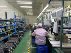
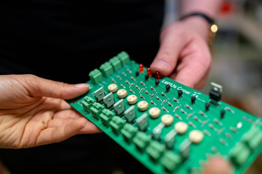
Building a PCB prototype involves attaching and soldering electronic components onto a manufactured printed circuit board (PCB) to create a working prototype. This step is critical for validating the functionality and reliability of the PCB design before moving into mass production. Different assembly techniques are used based on the type of components, board complexity, and production volume. In this section, we will cover the two main assembly techniques—Surface-Mount Technology (SMT) and Through-Hole Technology (THT)—and the equipment and methods used to ensure successful PCB assembly.
Surface-Mount Technology (SMT)
Surface-Mount Technology (SMT) is the most common method used in modern electronics assembly, particularly for high-density and compact PCBs. In SMT, components are placed directly onto the surface of the PCB rather than using leads that pass through holes. This method enables the use of smaller components and allows for higher circuit complexity in a compact space.
Process of SMT Assembly:
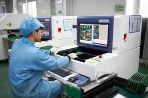
Solder Paste Application: The assembly process begins by applying solder paste to the PCB. This is typically done using a stencil to ensure that the solder paste is precisely applied only to the pads where components will be mounted. The solder paste consists of small particles of solder suspended in a flux medium.
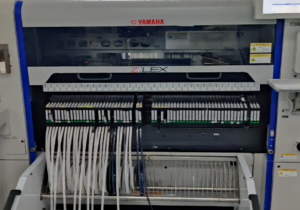
- Pick-and-Place: Once the solder paste is applied, a pick-and-place machine automatically places the surface-mount components (such as resistors, capacitors, and ICs) onto the corresponding pads on the PCB. These machines are highly accurate and can handle a wide variety of components quickly, which is essential for high-volume or complex boards.
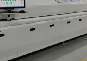
- Reflow Soldering: After the components are placed, the board is passed through a reflow oven. The oven heats the board to a temperature that melts the solder paste, causing it to bond the components to the copper pads on the PCB. The board is then cooled, solidifying the solder joints and securing the components in place.
Through-Hole Technology (THT)
Through-Hole Technology (THT) involves inserting component leads through holes drilled into the PCB and soldering them to pads on the opposite side. While this method is older than SMT, it is still widely used for certain types of components that require strong mechanical bonds, such as connectors, large capacitors, and components that need to handle high power.
Process of THT Assembly:
- Component Placement: In THT, components are placed manually or semi-automatically by inserting their leads through pre-drilled holes in the PCB. Components such as connectors, large resistors, and capacitors are often placed this way because they require more mechanical strength than surface-mounted components.
- Wave Soldering: For larger production runs, a process known as wave soldering is used. In wave soldering, the PCB passes over a wave of molten solder that coats the leads and the bottom pads of the PCB, forming solid electrical and mechanical connections. For smaller runs or prototypes, manual soldering is often used.
- Manual Soldering: In many cases, especially during the prototyping phase or for low-volume production, THT components are soldered manually using a soldering iron. Manual soldering is also used for rework and adjustments during the prototyping phase.
Mixed Technology (Hybrid Assembly)
In many cases, a PCB will require both SMT and THT components, especially when combining high-density, small components (SMT) with mechanically robust or high-power components (THT). This approach is known as mixed technology or hybrid assembly.
Hybrid Assembly Process:
- SMT First, Then THT: Typically, SMT components are placed and soldered first using the standard SMT process. After reflow soldering, THT components are added manually or semi-automatically, followed by wave soldering or manual soldering to complete the assembly.
- Optimized for Both Technologies: Hybrid assembly allows the designer to take advantage of the strengths of both technologies. For example, the high-density capabilities of SMT can be combined with the durability and power-handling capabilities of THT in one design.
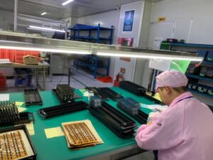
Manual Assembly Techniques
In low-volume prototyping or for boards with special requirements, manual assembly is often used. This technique involves placing components by hand and using a soldering iron to make connections. While time-consuming, manual assembly is often necessary during the prototyping phase to allow for flexibility and testing.
Manual Assembly Steps:
- Component Placement: Components are manually placed on the board using tweezers or pliers. SMT components may be held in place using solder paste until they can be soldered.
- Soldering: A soldering iron or hot air rework station is used to manually solder components. For SMT components, solder paste is applied first, and heat is used to reflow the solder. For THT components, traditional soldering techniques are used to attach leads to pads.
- Rework and Repair: Manual assembly also allows for easy rework and repairs. If a component needs to be replaced or repositioned, it can be desoldered and swapped out without significant disruption to the board.
Rework and Repair
During the assembly and prototyping process, it is common to encounter issues such as misplaced components, poor solder joints, or defective parts. Rework involves making corrections to the PCB after assembly to ensure the board functions correctly. This is especially important during the prototyping phase when designs may still be evolving.
Rework Techniques:
- Hot Air Rework: A hot air rework station is used to apply heat and remove or replace surface-mount components. This method is commonly used for reworking fine-pitch ICs and other sensitive components.
- Desoldering Pumps or Wick: These tools are used to remove excess solder or to clean up solder bridges between pads. Desoldering pumps suck up melted solder, while solder wick absorbs it through capillary action.
- Component Replacement: If a component is found to be faulty, it can be removed and replaced during rework. This is especially important for components that may have been damaged during initial assembly or testing.
Conclusion
PCB prototype assembly involves a range of techniques that vary depending on the type of components, the complexity of the design, and the production volume. Surface-Mount Technology (SMT) is ideal for high-density and automated production, while Through-Hole Technology (THT) offers mechanical strength for larger or power-handling components. Hybrid assembly combines both methods to optimize performance. Manual assembly is common during prototyping and allows for flexibility, though it is slower and more prone to error. Understanding these assembly techniques is key to successfully creating a functional PCB prototype that can be further tested and refined before moving to full production.
Chapter 8
Testing and Debugging
Testing and debugging are essential steps in the process of prototyping a PCB (Printed Circuit Board). These steps ensure that the prototype functions correctly and meets the design specifications before moving on to full-scale production. Testing is used to verify the electrical functionality, signal integrity, and overall performance of the board. Debugging involves identifying and resolving any issues that arise during testing, such as faulty connections, incorrect component values, or signal interference.
Visual Inspection
Before conducting any electrical tests, it is important to visually inspect the PCB. This step helps identify any obvious defects that could cause problems during testing, such as solder bridges, misaligned components, or damaged traces.
Solder Joint Inspection: Look for cold solder joints, which appear dull or cracked and can result in poor electrical connections. Any components that appear improperly attached may need to be reflowed or touched up.
Component Placement: Verify that all components are correctly placed and in their designated positions according to the PCB layout. Make sure that polarized components, such as diodes and capacitors, are installed in the correct orientation.
Trace Continuity: Check for any broken or damaged traces, as these can cause open circuits.
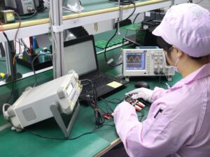
Electrical Testing
After completing the visual inspection, electrical testing should be performed to confirm that the PCB is functioning as intended. Electrical tests are used to check for continuity, short circuits, and correct voltage levels across the board.
- Continuity Testing: Use a multimeter to perform continuity tests to check for open circuits between traces, vias, and component connections. This ensures that there is an uninterrupted electrical path where there should be one.
- Power and Ground Checks: Before powering up the board, verify that the power and ground planes are properly connected and that there are no shorts between them. This is important to prevent damage to components when the board is powered.
- Voltage Measurements: Once the PCB is powered up, measure the voltage at key points (e.g., voltage regulators, IC power pins) to ensure that the correct operating voltages are present. This helps confirm that the power distribution network is functioning correctly.
Functional Testing
Functional testing ensures that the PCB operates as intended by simulating or replicating real-world operating conditions. This involves testing the PCB’s components, circuits, and overall functionality under normal operating conditions.
- Power-On Testing: After verifying the electrical integrity of the board, apply power and observe the board’s response. Check that key components, such as voltage regulators and microcontrollers, initialize correctly, and verify that power indicators (such as LEDs) behave as expected.
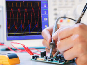
- Signal Integrity: For high-speed or high-frequency circuits, testing signal integrity is critical. Use an oscilloscope to examine waveforms at key points in the circuit. Ensure that signals are within expected voltage ranges and maintain proper timing, without excessive noise or distortion.
- Input/Output Functionality: Test the input/output (I/O) interfaces of the board, such as buttons, switches, connectors, and communication interfaces (e.g., USB, UART, SPI). Verify that data is being transmitted and received correctly.
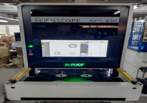
In-Circuit Testing (ICT)
In-Circuit Testing (ICT) is an automated testing method that checks the functionality of individual components and the integrity of connections on the PCB. ICT uses a “bed of nails” fixture to make contact with test points on the board, allowing for precise testing without requiring the entire board to be powered on.
- Component-Level Testing: ICT can test individual components, such as resistors, capacitors, diodes, and transistors, while they are still in-circuit. This ensures that all components are functioning correctly before performing system-wide tests.
- Connection Integrity: ICT can also verify that all solder joints are sound, checking for open circuits, shorts, and correct resistance levels between test points.
Debugging Techniques
When issues arise during testing, debugging is necessary to identify the root cause and correct the problem. Effective debugging involves systematic approaches to isolating and fixing faults.
- Isolating the Fault: Begin by identifying the section of the PCB where the issue is occurring. This can be done by testing one part of the circuit at a time, using the design schematics as a reference.
- Check for Incorrect Component Values: Ensure that all components are the correct values according to the Bill of Materials (BOM). Incorrect component values, such as resistors with the wrong resistance or capacitors with the wrong capacitance, can lead to improper circuit behavior.
- Reflow or Replace Faulty Components: If testing reveals faulty components (e.g., dead ICs, malfunctioning capacitors), these components can be desoldered and replaced. For SMT components, a hot air rework station is often used to safely remove and replace the components.
- Signal Probing: Use an oscilloscope or logic analyzer to probe specific points on the PCB and check the signal waveforms. Compare the actual signals to the expected ones to detect where things go wrong. For digital circuits, ensure that signals are correctly timed and free from noise.
Environmental Stress Testing
To ensure that the PCB prototype can withstand real-world environmental conditions, environmental stress testing is often performed. These tests simulate the conditions the PCB will experience during its operational life.
- Thermal Cycling: Subject the PCB to repeated cycles of extreme high and low temperatures to test for thermal expansion and contraction, which can cause stress on solder joints and components.
- Vibration Testing: Simulate vibration conditions that the PCB may encounter in environments like automotive, aerospace, or industrial applications. This tests the mechanical integrity of the solder joints and components.
- Humidity Testing: Expose the PCB to high humidity to check for potential moisture-related failures, such as corrosion or short circuits.
Final Verification and Validation
After completing the testing and debugging phases, conduct a final verification to ensure the prototype meets all performance, functionality, and reliability criteria. This step ensures the board is fully operational and ready for production.
- Functional Validation: Perform a full system test with all components operating simultaneously, and simulate real-world usage scenarios. Check for any remaining issues, such as signal degradation or component failures.
- Compliance Testing: Depending on the application, the PCB may need to comply with industry standards such as EMC (Electromagnetic Compatibility) testing, which checks for electromagnetic interference (EMI) or electrostatic discharge (ESD) protection.
Conclusion
Testing and debugging are critical stages in the PCB prototyping process that ensure the board functions as intended and meets design specifications. From initial visual inspections and continuity checks to advanced functional testing and signal analysis, each step plays a vital role in identifying potential issues. Systematic debugging and testing techniques, along with the right tools like oscilloscopes, multimeters, and logic analyzers, help ensure that the PCB prototype is ready for production, minimizing the risk of costly errors during full-scale manufacturing.
Chapter 9
Iteration and Refinement
Why is iteration important in PCB prototyping?
Because no PCB design is perfect on the first try. Iteration is a key part of the design process that allows engineers to identify and correct problems before moving into full production. Iteration helps in a number of ways:
- Identifying design flaws: The first prototype often reveals issues such as poor signal integrity, noise, or component placement problems that were not evident during the design phase. Iteration allows these flaws to be addressed before production.
- Improving performance: Through testing, engineers may find that certain aspects of the design, such as power distribution or thermal management, could be optimized. Iteration provides the opportunity to refine these areas for better performance.
- Ensuring manufacturability: Early prototypes help assess the manufacturability of the design. Iterating on the design ensures that it can be efficiently and cost-effectively manufactured at scale, avoiding problems in the production process.
- Enhancing reliability: Iterating on the prototype allows for the refinement of component choices, layout optimizations, and testing under real-world conditions to ensure long-term reliability of the final product.
Refining Your Design
Refining your design during PCB prototyping is all about making adjustments that make your board better. This can include:
- Optimizing Your Layout: Changing your layout to reduce noise, improve signal integrity, and make your board smaller.
- Choosing Better Components: Picking parts that work better, perform better, or cost less without sacrificing quality.
- Managing Heat: Making your board better at getting rid of heat by putting parts in better places or using materials that are better at conducting heat.
- Making Your Vias Better: Changing the size and placement of your vias to make your board more reliable and easier to build.
Testing is a critical part of this process. You need to test your board to make sure it does everything it’s supposed to do. You need to test it to make sure it can handle being used and abused. You need to test it to make sure it meets all the rules and regulations that apply to it. This is especially important if you’re going to sell your board or use it in a product that you’re going to sell.
Conclusion
The result of all this iteration and refinement is a board that’s ready to be used. It’s a board that you know will work, no matter what you throw at it. It’s a board that you can use in your product without worrying about it breaking or not working right. It’s a board that you can sell to someone else, knowing that they’ll be happy with it and that it won’t come back to you as a return.
Ultimately, the iteration and refinement process in PCB prototyping is all about making sure your board is as good as it can be. It’s about making sure your board meets the highest standards of quality and reliability before you start making a bunch of them.
Chapter 10
Finalizing the Design for Production
In the realm of printed circuit board (PCB) development, finalizing the design for production is a decisive phase that transitions a prototype into a ready-to-manufacture product. This stage is critical because it integrates all prior design refinements and testing insights into the final design, ensuring the PCB is optimized for mass production.
Essential Steps in Finalization
Design Verification: Before final production, the PCB design must undergo a thorough verification process to ensure it meets all specifications. This includes checking for any design errors such as incorrect footprint assignments, spacing issues, or potential short circuits. Tools like Design Rule Check (DRC) and Layout Versus Schematic (LVS) are used extensively to automate some of these verifications.
Optimization for Manufacturability: Adjustments are often made to the PCB design to make it easier and more cost-effective to produce. This may involve altering the layout to better suit the capabilities of manufacturing equipment, optimizing the placement of components to enhance performance and reduce waste, or tweaking the design to simplify assembly and testing processes.
Final Material Selection: Material choices are finalized based on performance requirements, cost, and availability. For PCBs, this includes selecting the substrate material, copper thickness, solder mask, and any other specialized coatings or finishes that are necessary for the intended application.
Prototype Testing: Although prototypes have been tested throughout the design process, final prototype testing is crucial to ensure that all changes and refinements have successfully eliminated previous issues without introducing new ones. This includes functional testing to verify that the PCB performs as expected under normal and extreme conditions.
Documentation and Release to Manufacturing: Comprehensive documentation is prepared and reviewed. This documentation includes final design files, assembly diagrams, and specifications. It’s crucial for ensuring that the manufacturing team has all the necessary information to produce the PCB accurately and efficiently.
Conclusion
Once the design is finalized, it’s released for production. This release marks the end of the prototyping phase and the beginning of manufacturing. At this point, the design should be fully optimized for scalability, cost-effectiveness, and reliability, ensuring a smooth transition into mass production and market deployment.
Finalizing the PCB design for production is a meticulous process that bridges the gap between prototype and full-scale production, ensuring that the final product is of the highest quality and ready for consumer use.
Get in touch
Where Are We?
Industrial Park, No. 438 Donghuan Road, No. 438, Shajing Donghuan Road, Bao'an District, Shenzhen, Guangdong, China
Floor 4, Zhihui Creative Building, No.2005 Xihuan Road, Shajing, Baoan District, Shenzhen, China
ROOM A1-13,FLOOR 3,YEE LIM INDUSTRIAL CENTRE 2-28 KWAI LOK STREET, KWAI CHUNG HK
service@southelectronicpcb.com
Phone : +86 400 878 3488
Send us a message
The more detailed you fill out, the faster we can move to the next step.


