
SMT Assembly Services
South-Electronic
Choose South-Electronic, you’ll experience unmatched quality and precision from start to finish.
Partner with South-Electronic today, and let us help you take your projects to the next level with innovative, high-quality!
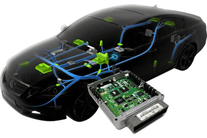
Your Trusted Supplier of SMT PCB Assembly
Welcome to South-Electronic, where you’ll find top-quality SMT PCB Assembly services known for their precision and reliability.
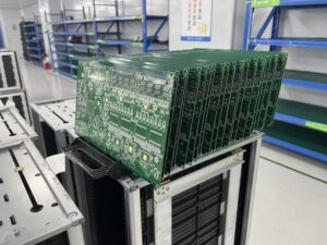
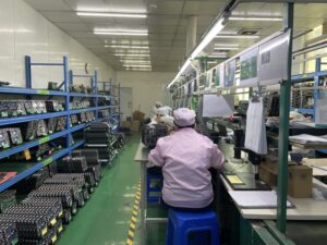
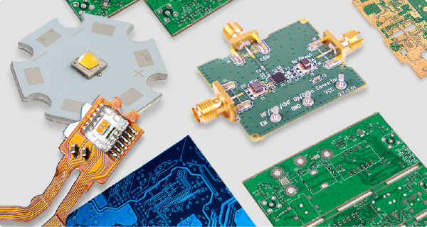
Our SMT PCB assemblies deliver excellent performance, making them perfect for a wide range of applications. Choose from single-layer, double-layer, and multi-layer boards, all customized to meet your specific electronic needs. Whether you’re improving efficiency in consumer electronics or need dependable operation in industrial controls, our SMT PCB Assembly services excel at delivering efficiency and precision. Count on South-Electronic for exceptional quality and consistency in your electronic endeavors. Our SMT PCB assemblies enhance your devices’ functionality with superior reliability and performance. Partner with us for excellence and innovation in your field.
Single-Sided SMT Assembly
Single-sided SMT assembly is when you put components on one side of the board. It's good for simpler, cheaper designs where you don't need as many components. It's used a lot in basic electronic devices because it's cheap and easy to make.
Double-Sided SMT Assembly
Double-sided SMT assembly is when you put components on both sides of the board. This lets you put more components on the board and do more things with it. It's good for more complicated designs that need more space for components and it's better for more advanced electronics.
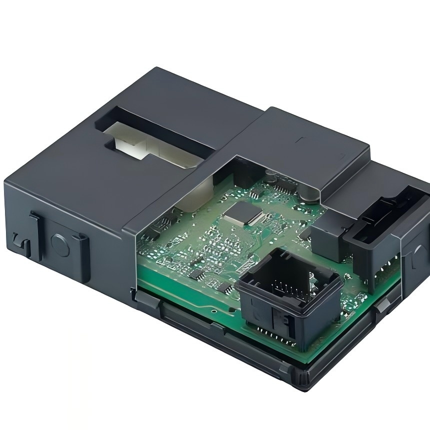
Ball Grid Array (BGA) Assembly
BGA assembly is when you use a grid of solder balls to connect components to the board. It's good for high-density, high-performance circuits like CPUs and GPUs. BGA gives you better electrical performance and better heat dissipation, so it's good for advanced technology devices that need small, reliable connections.
Why Choose South-Electronic?
Choose South-Electronic for our expertise in custom, high-quality SMT Assembly services for a wide range of applications. Our team has extensive experience, which means we can provide superior quality at competitive prices and exceptional service from start to finish.
- Precision and Quality
Your project deserves nothing but the highest standards. At South-Electronic, we ensure precision and reliability in every SMT assembly we produce, guaranteeing that your products are flawless and perform exactly as expected.
- Flexible Customization
We tailor our services to meet your specific requirements, whether you need single-sided, double-sided, or BGA assembly. Whatever your needs are, you can scale your orders with flexibility, all while maintaining uncompromising quality.
- Fast Turnaround
We understand that time is crucial for your business. That’s why our highly efficient production lines ensure you receive your orders quickly, helping you stay ahead of your deadlines and keep your projects on track.
- Experienced Team
When you work with us, you're supported by a team with years of experience in PCB assembly. You’ll benefit from the confidence of working with professionals who understand your industry and know how to meet your specific needs.
- One-Stop Solution
From initial design to final assembly, we take care of every step in the process. With us, you get the convenience of a full-service partner who can handle all your PCB needs seamlessly, giving you peace of mind and simplifying your workflow.
- No Minimum Order Requirements
You have the freedom to order exactly what you need, no matter how small the quantity. Even if it’s just a single unit, we are here to meet your requirements with no minimum order constraints, giving you complete flexibility in your purchasing decisions.
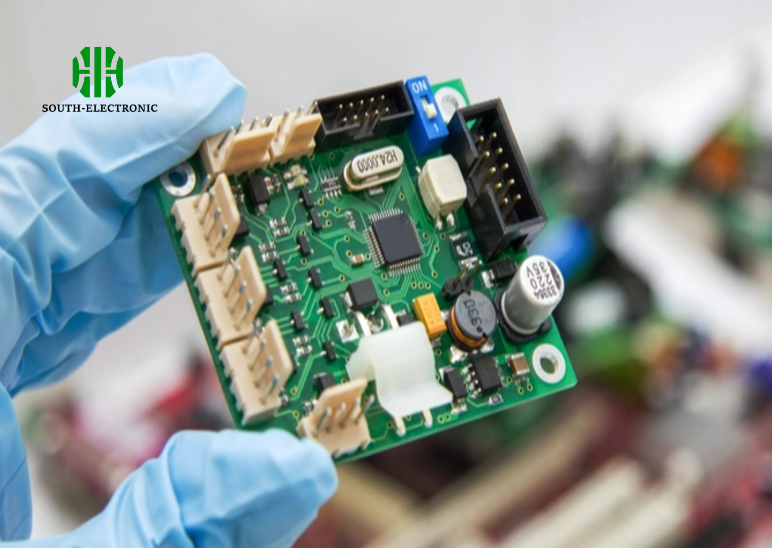
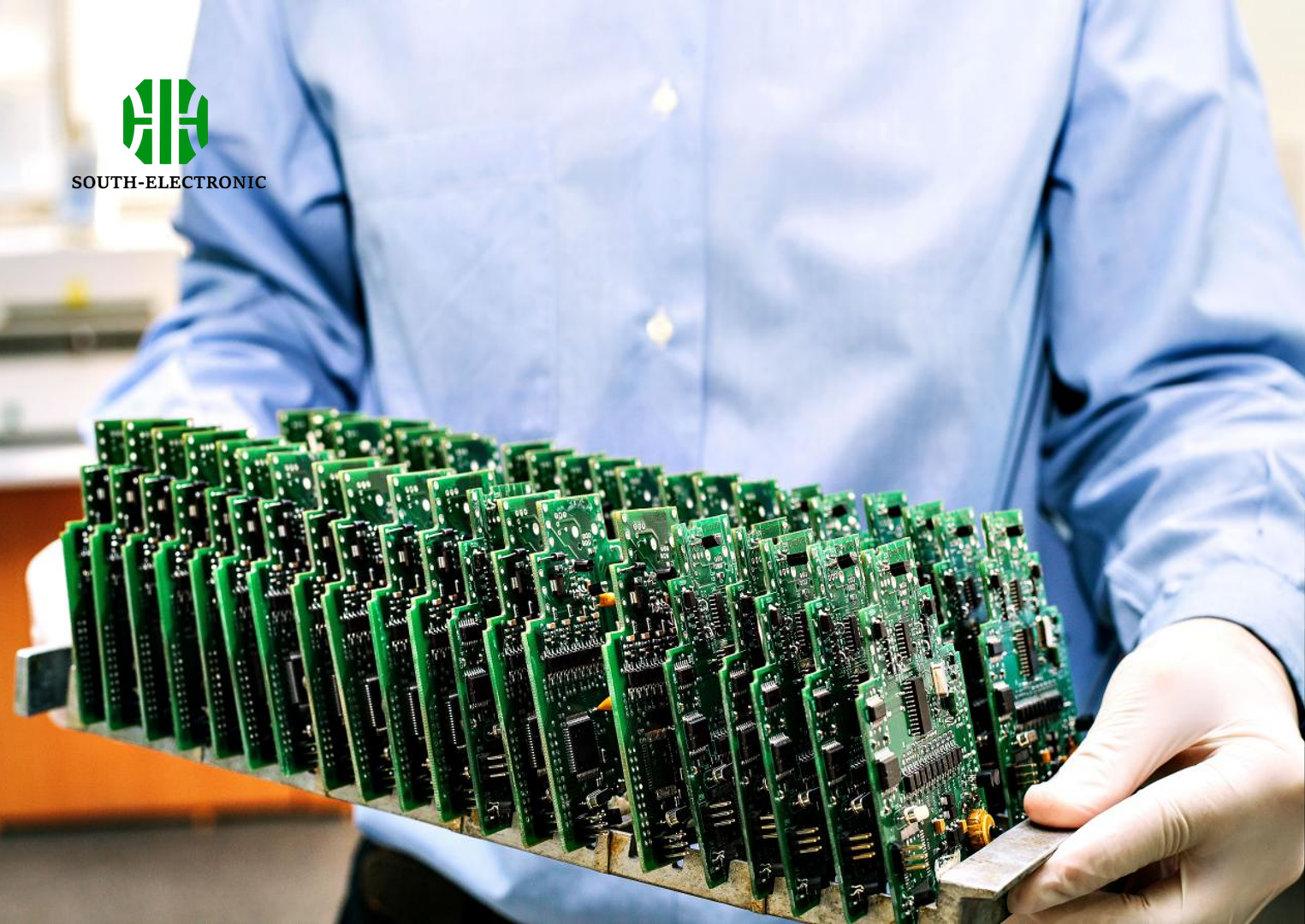
Related Project We had Done
Customer Reviews
engineer
thank you, guys, the boards are really good, i am really happy to receive my boards, the components are perfect!

Operation Manager
South-Electronic is my first PCBA supplier in China. The service and quality are excellent, and the after-sales support is also very impressive. Good Job!

Common Questions
Most Popular Questions
South-Electronic specializes in assembling a wide range of PCBs, including single-sided, double-sided, and multi-layer boards, as well as Ball Grid Array (BGA) assemblies. They cater to various industries and can handle both simple and complex designs.
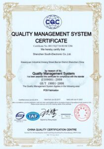
South-Electronic follows strict quality control processes throughout the SMT assembly. They use advanced equipment and conduct thorough inspections at every stage, ensuring that each assembly meets precise standards. They are also ISO9001 certified, which adds another layer of assurance in terms of quality and reliability.
The typical delivery timeline varies depending on the complexity and quantity of the order. However, South-Electronic prides itself on offering fast turnaround times, usually completing most projects within a few weeks, while also providing expedited services for urgent orders.
To get an accurate quote, you'll need to provide detailed information such as your PCB design files (Gerber files), Bill of Materials (BOM), quantity, and any specific assembly requirements. The more precise your information, the more tailored the quote will be.
South-Electronic holds ISO9001 certification, demonstrating their commitment to quality management and production standards. They ensure precision and reliability through rigorous testing, state-of-the-art equipment, and experienced technicians who oversee every aspect of the assembly process.
South-Electronic offers comprehensive after-sales support, including a warranty on their SMT assemblies. They typically provide up to a five-year warranty, ensuring customers are covered for any potential defects or issues. Their customer service team is always available to assist with any after-sales concerns.
Send us a message
The more detailed you fill out, the faster we can move to the next step.


The Complete Guide for SMT Assembly
Contents
Chapter 1
Introduction to SMT Assembly
Surface Mount Technology (SMT) is a way to make electronic circuits. Instead of putting the parts through holes in the circuit board, the parts are put on the surface of the board. This makes the circuit board smaller and better. SMT is used to make all kinds of electronics, like phones, computers, and other things we use every day. It is the best way to make electronics because it makes them smaller, faster, and cheaper.
SMT is better than the old way of making electronics because it makes the parts smaller. The parts in SMT are called Surface Mount Devices (SMDs). They are a lot smaller than the old parts. This means the electronics can be smaller. SMT also makes the parts faster. The parts are put on the board by a machine, so it is faster than doing it by hand. SMT also makes the parts cheaper. The machine can put the parts on the board faster and more times than a person can. This makes the parts cheaper. SMT is the best way to make electronics because it makes them smaller, faster, and cheaper.
SMT is the best way to make electronics because it makes them smaller. The parts in SMT are smaller than the old parts. This means the electronics can be smaller. SMT is the best way to make electronics because it makes them faster. The parts are put on the board by a machine, so it is faster than doing it by hand. SMT is the best way to make electronics because it makes them cheaper. The machine can put the parts on the board faster and more times than a person can. This makes the parts cheaper. SMT is the best way to make electronics because it makes them smaller, faster, and cheaper.
Chapter 2
How SMT Assembly Works
SMT assembly is a highly automated process used to attach surface-mount devices (SMDs) directly to the surface of a printed circuit board (PCB). Here’s a step-by-step explanation of how SMT assembly works and the key components involved:
Step 1: Apply Solder Paste
The process starts with applying solder paste to the PCB. A stencil is placed over the board to ensure that the paste is applied only to the areas where components will be mounted. The solder paste, a combination of tiny solder balls and flux, acts as an adhesive to hold the components in place before soldering and creates electrical connections between the component leads and the PCB pads.
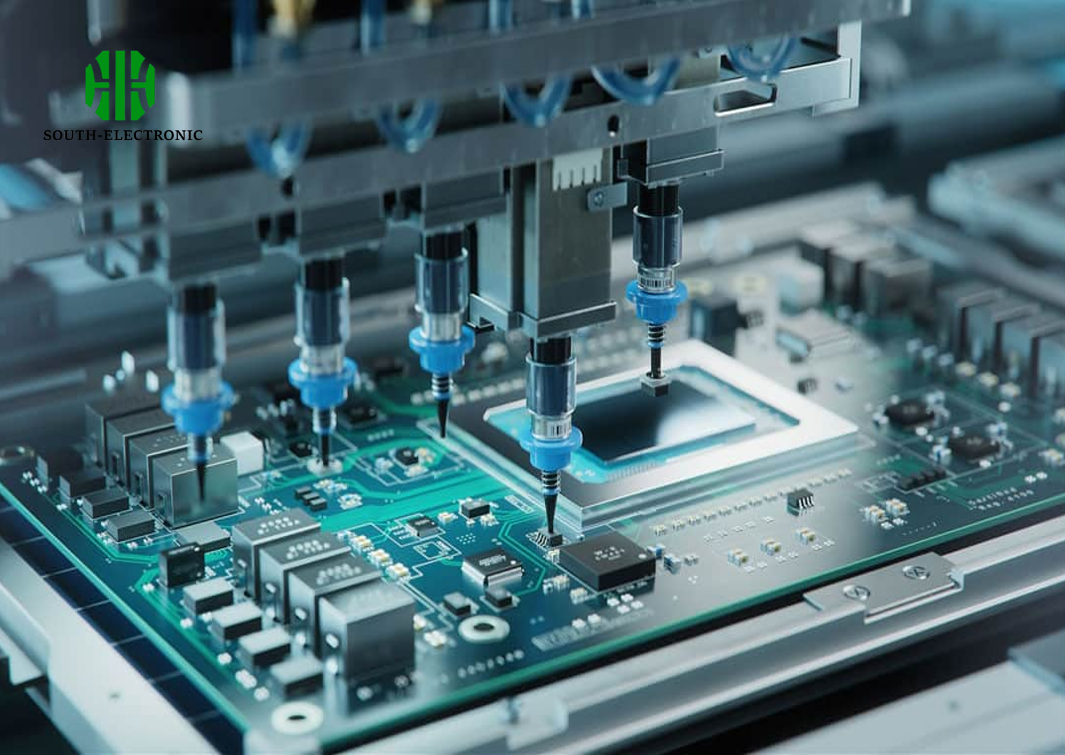
Step 2: Pick-and-Place Machines
Once the solder paste is applied, the PCB is passed to a pick-and-place machine. This highly precise machine picks up the tiny surface-mount components from reels or trays and places them on the PCB according to the design layout. Modern pick-and-place machines are capable of placing thousands of components per hour, ensuring speed and accuracy.
Step 3: Reflow Soldering
After the components are placed on the board, the assembly moves into the reflow oven. Here, the PCB is heated to a specific temperature, causing the solder paste to melt and form solid solder joints. The reflow process is carefully controlled to ensure that the solder melts and solidifies without damaging the components or the PCB itself. Once the board cools down, the components are firmly attached, and electrical connections are established.
Step 4: Inspection and Testing
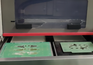
Once the soldering process is complete, the PCB undergoes inspection to ensure proper assembly. Automated Optical Inspection (AOI) machines scan the board to check for missing components, soldering defects, and misalignments. In some cases, X-ray inspection may also be used, particularly for complex assemblies like Ball Grid Array (BGA) packages where solder joints are hidden beneath the component.
Key Components Involved in SMT Assembly
- Solder Paste: A combination of flux and fine solder particles that temporarily holds the components in place and eventually creates the solder joints during reflow.
- Pick-and-Place Machine: Automated equipment that places components onto the PCB with high precision, handling even the tiniest SMDs.
- Reflow Oven: A specialized oven that heats the PCB to melt the solder paste and securely attach the components to the board.
- Stencil: A template used to apply solder paste accurately to specific areas of the PCB.
Chapter 3
Types of SMT Assembly
SMT assembly comes in different forms depending on the complexity and requirements of the PCB design. The main types include single-sided, double-sided, and multi-layer SMT assemblies, each offering unique advantages in terms of space utilization, functionality, and performance. Additionally, advanced assembly techniques such as Ball Grid Array (BGA) and Chip-on-Board (COB) provide specialized solutions for high-performance electronics.
Single-Sided SMT Assembly
Single-sided SMT assembly involves mounting all components on one side of the PCB. This type of assembly is typically used in simpler, cost-effective designs where fewer components are needed, making it ideal for basic electronics. It is widely used in consumer products like home appliances, remote controls, and basic electronic gadgets. Single-sided SMT assembly is preferred when the design is straightforward, space is not a major constraint, and the functionality requirements are relatively low.
- Advantages: Low cost, easier manufacturing, suitable for simple designs.
- Applications: Basic electronics, entry-level devices, and low-density circuits.
Double-Sided SMT Assembly
In double-sided SMT assembly, components are mounted on both sides of the PCB, allowing for greater component density and increased functionality. This type of assembly is ideal for more complex electronics where more components are needed but space is limited. Double-sided SMT allows designers to make efficient use of both surfaces of the PCB, optimizing the layout and enhancing the overall performance of the product.
- Advantages: Higher component density, more functionality, efficient use of space.
- Applications: Telecommunication devices, medical equipment, industrial control systems, and other compact, high-performance electronics.
Multi-Layer SMT Assembly
Multi-layer SMT assembly involves the use of PCBs with multiple layers of conductive pathways stacked together, separated by insulating layers. This allows for even greater component density and more complex designs, enabling higher performance without increasing the size of the board. Multi-layer SMT is essential for devices that require advanced functionality, high-speed data processing, or high signal integrity in a compact form factor.
- Advantages: Supports complex, high-performance designs, reduces electromagnetic interference, and allows for faster data transmission.
- Applications: Smartphones, laptops, advanced communication systems, and aerospace electronics.
Ball Grid Array (BGA) Assembly
BGA assembly is a specialized form of SMT where components are mounted using a grid of small solder balls on the underside of the component. BGA offers several benefits over traditional SMT methods, including better electrical performance, improved thermal dissipation, and the ability to handle a high density of connections in a compact area. BGA is commonly used for components like processors, GPUs, and memory chips, where performance and reliability are critical.
- Advantages: Enhanced electrical performance, improved heat dissipation, supports high-density connections.
- Applications: CPUs, GPUs, memory modules, and other high-performance computing components.
Chip-on-Board (COB) Technology
Chip-on-Board (COB) is an advanced packaging method where bare semiconductor chips are mounted directly onto the PCB and wire-bonded to the board’s circuitry. The chips are then encapsulated with a protective layer, usually an epoxy resin, to shield them from environmental factors. COB technology is advantageous for applications requiring compact designs and high-performance characteristics, as it reduces the number of intermediate packaging steps, lowering the cost and size of the assembly.
- Advantages: Smaller footprint, lower cost, and improved reliability due to fewer connections.
- Applications: LED lighting, sensors, compact electronic modules, and consumer electronics.
Summary
Each type of SMT assembly—whether single-sided, double-sided, or multi-layer—serves different design needs based on the complexity, size, and performance requirements of the product. BGA and COB technologies are advanced methods that enhance performance in high-density, high-speed applications. These various SMT assembly types allow manufacturers to build increasingly compact, powerful, and reliable electronic products across a wide range of industries.
Chapter 4
Advantages of SMT Over Through-Hole Technology
SMT and through-hole technology are the two primary methods for assembling electronic components onto printed circuit boards (PCBs). Through-hole technology, which involves inserting component leads into pre-drilled holes on the PCB, was once the standard but has largely been replaced by SMT due to its many advantages in terms of efficiency, performance, and cost. Here’s a detailed comparison of SMT vs. through-hole assembly, along with the key benefits SMT offers.
Comparison of SMT vs. Through-Hole Assembly
1.Component Mounting
- Through-Hole Assembly: Components in through-hole technology have leads that are inserted into drilled holes on the PCB and then soldered on the opposite side of the board. This creates a mechanically strong connection, making through-hole technology ideal for components that will experience mechanical stress or are subject to frequent movement.
- SMT Assembly: In contrast, SMT components are placed directly onto the surface of the PCB without the need for drilling. These surface-mounted devices (SMDs) are smaller, lighter, and easier to handle in automated assembly processes.
2.Space Utilization
- Through-Hole Assembly: Through-hole technology requires more space on the PCB due to the size of components and the need for drilled holes. This limits the density of components and makes it harder to create compact designs.
- SMT Assembly: SMT allows for much greater component density because components can be placed directly on the surface of the board, and they can be mounted on both sides of the PCB. This is especially important for modern electronics that require compact, lightweight designs.
3.Assembly Speed
- Through-Hole Assembly: Through-hole assembly tends to be slower and more labor-intensive, as each component must be inserted into the PCB by hand or by semi-automated machines. The drilling process also adds extra time to the manufacturing cycle.
- SMT Assembly: SMT is highly automated, using pick-and-place machines to position components with high speed and precision. This automation significantly reduces assembly time and increases production throughput, making SMT the preferred method for high-volume manufacturing.
4.Cost Efficiency
- Through-Hole Assembly: The additional steps required in through-hole assembly, such as drilling holes and manual placement of components, lead to higher production costs. Furthermore, through-hole components are generally larger and more expensive than surface-mount components.
- SMT Assembly: SMT is more cost-effective due to its automation, faster assembly times, and the use of smaller, cheaper components. With fewer manual processes involved and the ability to handle high-volume production efficiently, SMT lowers overall manufacturing costs.
5.Mechanical Strength
- Through-Hole Assembly: Through-hole components provide better mechanical strength because the leads go through the board and are soldered on the other side. This makes it suitable for connectors or components that are subject to physical stress or require durability, such as transformers or large capacitors.
- SMT Assembly: While SMT components are more compact, they do not provide the same mechanical strength as through-hole components. However, for most electronic applications, where size, speed, and efficiency are prioritized, the mechanical strength of SMT is sufficient.
Key Benefits of SMT Over Through-Hole Technology
1.Space Efficiency
Space Efficiency One of the major advantages of SMT is its ability to fit more components on a single board due to the smaller size of surface-mount devices (SMDs). This allows for higher-density designs and more functionality in smaller spaces. Devices like smartphones, wearables, and tablets all benefit from the compact nature of SMT assemblies, where space is at a premium.
2.Space Efficiency
Higher Assembly Speed SMT allows for faster assembly because the process is almost entirely automated. Machines such as pick-and-place systems can position components quickly and accurately, handling thousands of components per hour. This results in shorter production times and the ability to meet high-volume demands, which is essential for consumer electronics and other mass-produced products.
3.Space Efficiency
Cost Savings SMT assembly generally costs less than through-hole assembly for several reasons:
- No drilling: SMT eliminates the need for drilling holes in the PCB, which reduces production costs and speeds up the manufacturing process.
- Smaller components: SMDs are typically smaller and cheaper than through-hole components, allowing manufacturers to save on materials.
- Automation: The high level of automation in SMT leads to lower labor costs and faster production cycles, reducing overall costs per unit.
4.Design Flexibility
Design Flexibility With SMT, components can be mounted on both sides of the PCB, enabling designers to create more complex and multifunctional boards. This flexibility is especially useful for advanced electronic devices that require high levels of functionality within limited space. SMT also allows for more innovative designs and smaller, lighter products, making it the technology of choice for portable electronics.
5.Improved Performance
Improved Performance SMT assemblies tend to have better electrical performance because the shorter leads used in SMDs reduce parasitic effects like inductance and resistance. This leads to higher operating speeds and better signal integrity, which is crucial for high-frequency and high-speed circuits.
6.Enhanced Thermal Dissipation
Enhanced Thermal Dissipation SMDs are more efficient at dissipating heat compared to through-hole components. The close contact between the component and the PCB surface allows for better thermal transfer, which is especially beneficial in applications that generate a lot of heat, such as power electronics and processors.
Conclusion
While through-hole technology still has specific applications, particularly for components that need mechanical strength or are exposed to physical stress, SMT offers clear advantages in terms of space efficiency, assembly speed, cost savings, and overall performance. As a result, SMT has become the preferred choice for most modern electronics, from consumer gadgets to industrial and medical devices, thanks to its ability to deliver high-density, high-performance, and cost-effective solutions.
Chapter 5

SMT Assembly Equipment and Tools
SMT assembly is a highly automated and precise process that requires specialized equipment to ensure efficiency, accuracy, and high-quality results. The key to successful SMT assembly lies in the use of advanced technology, which allows for the rapid and accurate placement of tiny components on the surface of a printed circuit board (PCB). In this section, we will explore the essential equipment and tools used in the SMT assembly process and how they contribute to improved precision and efficiency.
1. Solder Paste Printer
The solder paste printer is the first piece of equipment used in the SMT assembly process. It applies solder paste—a mixture of fine metal solder particles and flux—onto the surface of the PCB where the components will be placed. A stencil, which is a thin metal sheet with openings corresponding to the pads on the PCB, is used to control the exact placement and thickness of the solder paste.
- Purpose: Ensures accurate application of solder paste to specific areas of the PCB where components will be mounted.
- Importance: A precise and uniform solder paste application is critical for creating strong, reliable solder joints during the reflow process.
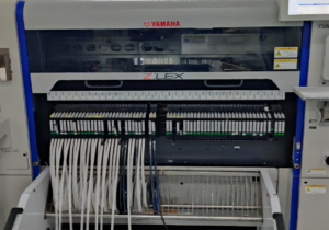
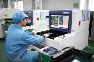
2. Pick-and-Place Machine
The pick-and-place machine is one of the most crucial pieces of equipment in SMT assembly. This highly automated machine is responsible for picking up surface-mount components from reels or trays and accurately placing them onto the PCB. Modern pick-and-place machines use robotic arms with suction or tweezers to handle even the tiniest components, positioning them with high precision at incredibly fast speeds.
- Purpose: Places SMDs (Surface Mount Devices) onto the PCB at their designated locations according to the design file.
- Importance: The speed and precision of the pick-and-place machine are key to the overall efficiency of the SMT process. With modern machines capable of placing thousands of components per hour, they significantly reduce assembly time while maintaining exceptional accuracy.
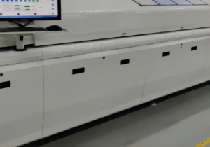
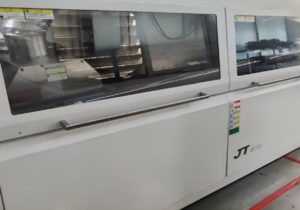
3. Reflow Oven
After the components are placed on the PCB, the entire assembly goes through a reflow oven. This specialized oven heats the board to a temperature high enough to melt the solder paste, allowing it to flow and create strong electrical and mechanical connections between the components and the PCB. The reflow oven uses carefully controlled temperature profiles to ensure that the solder melts and cools evenly without damaging sensitive components.
- Purpose: Heats the PCB to melt the solder paste and form solid solder joints between the components and the PCB pads.
- Importance: Reflow soldering is a critical step in the SMT process, ensuring the components are securely attached and electrically connected. Proper temperature control in the reflow oven is essential to prevent issues like solder bridging or component damage.
4. Automated Optical Inspection (AOI)
Automated Optical Inspection (AOI) systems are used to inspect the PCB after reflow soldering. AOI machines use high-resolution cameras and advanced algorithms to scan the PCB and detect any defects such as missing components, misalignments, poor solder joints, or other inconsistencies. This inspection process helps identify issues early in the production cycle, reducing the need for costly rework.
- Purpose: Inspects PCBs for defects, such as misaligned components or soldering issues, after the reflow process.
- Importance: AOI provides an efficient, non-contact method to ensure the quality of SMT assemblies, minimizing the chances of faulty boards being shipped to customers.
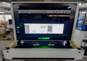
5. X-ray Inspection System
For complex assemblies, such as those involving Ball Grid Array (BGA) components, an X-ray inspection system is often used. Since the solder joints in BGA components are hidden beneath the package, traditional optical inspection methods are insufficient. X-ray inspection allows manufacturers to examine the internal structure of solder joints, identifying hidden defects like voids or cracks.
- Purpose: Inspects hidden solder joints, particularly in BGA and other components where visual inspection is not possible.
- Importance: X-ray inspection ensures that even hidden solder joints are properly formed, providing greater assurance of the assembly’s reliability and functionality.
6. Stencil Printer
The stencil printer is used in the early stages of SMT assembly to apply solder paste accurately to the PCB. The stencil is a thin sheet of metal with cutouts corresponding to the pads on the PCB where the solder paste needs to be applied. The stencil printer ensures that the solder paste is applied in precise amounts to each pad, which is essential for forming strong, reliable solder joints during reflow.
- Purpose: Applies solder paste to the PCB in a controlled manner using a stencil.
- Importance: Ensures that solder paste is deposited only where it’s needed, in the right amounts, ensuring optimal solder joints in the final product.
7. Solder Paste Inspection (SPI) System
A Solder Paste Inspection (SPI) system is used to check the quality and consistency of the solder paste applied to the PCB. This machine measures the height, volume, and alignment of the solder paste to ensure it meets the required specifications before components are placed on the board.
- Purpose: Verifies the quality and consistency of the solder paste application.
- Importance: Ensures proper soldering by confirming that the correct amount of solder paste has been applied to each pad, reducing defects caused by poor solder coverage.
8. Rework Station
Even with high levels of automation, errors or defects can occasionally occur. A rework station is used to manually remove and replace faulty components or repair soldering issues. It is equipped with tools like hot air guns, tweezers, and soldering irons to allow technicians to correct errors without damaging the PCB or other components.
- Purpose: Allows manual correction of errors, such as replacing defective components or fixing soldering issues.
- Importance: Provides a way to address minor defects without discarding the entire board, improving cost-efficiency and reducing waste.
How Technology Enhances Precision and Efficiency in SMT Assembly
Modern technology plays a pivotal role in the precision and efficiency of SMT assembly. The use of highly automated equipment, such as pick-and-place machines and reflow ovens, ensures that even the smallest and most intricate components are placed and soldered with extreme accuracy. This automation not only speeds up the manufacturing process but also reduces the risk of human error, leading to higher-quality products and fewer defects.
In addition, advanced inspection systems like AOI and X-ray machines help detect defects early in the production process, ensuring that only fully functional and reliable PCBs are delivered to customers. By integrating cutting-edge technology, SMT assembly lines can produce high-volume, high-quality assemblies at a fraction of the time and cost compared to manual methods.
Conclusion
The SMT assembly process relies on a variety of sophisticated equipment and tools that work together to achieve fast, accurate, and cost-effective production. From solder paste printers and pick-and-place machines to reflow ovens and inspection systems, each piece of equipment plays a crucial role in ensuring the success of SMT assembly. As technology continues to evolve, the precision and efficiency of SMT assembly will only improve, making it the preferred choice for modern electronics manufacturing.
Chapter 6
Common Challenges in SMT Assembly
While Surface Mount Technology (SMT) assembly has revolutionized the electronics manufacturing industry by improving efficiency, reducing costs, and allowing for more compact designs, the process is not without its challenges. Various issues can arise during SMT assembly that can affect the quality, functionality, and reliability of the final product. Here, we will discuss some of the typical issues encountered during the SMT process, such as solder defects and component misalignment, and explore solutions and best practices to overcome these challenges.
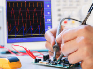
1. Solder Defects
Soldering is one of the most critical stages in the SMT assembly process, as it forms the electrical and mechanical connection between the surface-mount components and the PCB. However, various solder defects can occur during the reflow process, which can compromise the quality of the assembly.
Common Solder Defects:
- Solder Bridging: Occurs when excess solder creates a bridge between two adjacent pads or component leads, leading to short circuits.
- Insufficient Solder: When too little solder is applied, it can result in weak solder joints, which may cause intermittent or complete failure of the electrical connection.
- Solder Voids: Air bubbles trapped within the solder joint, known as voids, can reduce the mechanical strength and thermal conductivity of the joint, potentially leading to component failure.
- Tombstoning: When one end of a small component lifts up during reflow, it forms a “tombstone” shape, leaving one side of the component disconnected.
Solutions and Best Practices for Solder Defects:
- Solder Paste Application: Ensuring consistent and accurate solder paste application is crucial to preventing defects. Using high-quality stencils and maintaining proper alignment between the stencil and PCB can help avoid issues like solder bridging and insufficient solder.
- Reflow Oven Profile: Properly controlling the reflow oven temperature profile is key to reducing defects like tombstoning and solder voids. The temperature must be carefully ramped up and down to ensure even solder melting and cooling without causing thermal stress to the components.
- Solder Paste Quality: Using high-quality solder paste with the correct viscosity and composition ensures better adhesion, reduces voids, and improves the overall quality of the solder joints.
2. Component Misalignment
Component misalignment occurs when surface-mount components are not placed correctly on their designated pads. This issue can lead to electrical failures, poor mechanical connections, or problems during reflow soldering.
Causes of Component Misalignment:
- Pick-and-Place Errors: The automated pick-and-place machine may misplace components due to calibration issues, improper settings, or mechanical problems.
- PCB Warping: If the PCB is warped or bent, components may not align properly with the pads, leading to poor connections.
- Solder Paste Misalignment: Misaligned solder paste can shift the component placement, resulting in solder defects or weak connections.
Solutions and Best Practices for Component Misalignment:
- Pick-and-Place Machine Calibration: Regularly calibrate and maintain the pick-and-place machine to ensure precise component placement. Ensuring that the machine is programmed correctly and that the nozzles and suction cups are functioning properly can reduce errors.
- PCB Flatness: Ensuring the PCB is flat and free from warping before assembly is crucial. Using high-quality PCB materials and storing them in appropriate conditions can help prevent warping.
- Visual Inspection: Before reflow, conduct visual or Automated Optical Inspection (AOI) to detect any misaligned components. This allows for corrections before the soldering process, saving time and reducing rework.
3. Tombstoning
Tombstoning occurs when a small passive component, such as a resistor or capacitor, lifts up from one end during the reflow process. This leaves one side of the component unconnected to the PCB, causing an open circuit. Tombstoning is more common with smaller components, like 0201 or 0402 packages.
Causes of Tombstoning:
- Uneven Heating: If one side of the component heats up faster than the other during reflow, the solder on the hotter side will melt first and pull the component upwards.
- Solder Paste Imbalance: If the solder paste is not applied evenly, it can cause uneven forces during reflow, leading to tombstoning.
Solutions and Best Practices for Tombstoning:
- Reflow Profile Optimization: Ensure a uniform reflow oven temperature profile that heats both ends of the component simultaneously, reducing the risk of tombstoning.
- Stencil Design: Using a well-designed stencil that applies even amounts of solder paste to both pads can prevent imbalances that lead to tombstoning.
4. Solder Balling
Solder balling occurs when small balls of solder form on the PCB instead of flowing evenly to form a proper joint. These solder balls can cause short circuits or lead to unreliable solder connections.
Causes of Solder Balling:
- Excess Solder Paste: Applying too much solder paste can result in excess solder spreading and forming balls during reflow.
- Moisture in PCB or Solder Paste: If the PCB or solder paste contains moisture, it can cause solder spattering during reflow, leading to solder balls.
Solutions and Best Practices for Solder Balling:
- Control Solder Paste Amount: Use the correct amount of solder paste, applied with a properly designed stencil. Ensure the stencil apertures are correctly sized to prevent excessive paste application.
- Dry Storage: Store PCBs and solder paste in dry conditions to prevent moisture absorption. Pre-baking PCBs before reflow can also help eliminate any moisture that could cause solder spattering.
5. Insufficient Solder Wetting
Solder wetting refers to the ability of the solder to flow and adhere to the component leads and PCB pads. Insufficient wetting can result in weak solder joints, which may fail under mechanical or thermal stress.
Causes of Insufficient Solder Wetting:
- Contaminated PCB or Components: Oxidation or contamination on the PCB pads or component leads can prevent proper solder adhesion.
- Low Soldering Temperature: If the reflow oven temperature is too low, the solder may not fully melt, leading to poor wetting.
Solutions and Best Practices for Insufficient Solder Wetting:
- Surface Cleaning: Ensure that both the PCB and components are free from contaminants like dust, oil, or oxidation. Using a protective coating on PCBs during storage can help prevent oxidation.
- Optimal Reflow Temperature: Ensure that the reflow oven is set to the correct temperature profile to allow the solder to melt fully and wet the surfaces effectively.
6. Component Damage
During SMT assembly, components can be damaged due to excessive heat, physical handling, or improper storage. Damaged components can lead to assembly failures or reduced product reliability.
Causes of Component Damage:
- Excessive Reflow Heat: If the reflow oven temperature is too high or the board spends too long in the oven, sensitive components can be damaged.
- Mechanical Handling: Improper handling of components during the pick-and-place process or during storage can result in physical damage.
Solutions and Best Practices for Component Damage:
- Reflow Profile Control: Use a carefully controlled reflow temperature profile to avoid overheating components.
- Proper Handling Procedures: Implement best practices for handling components, including proper storage in ESD-safe environments and using automated equipment to minimize physical contact.
Conclusion
SMT assembly is a highly efficient process, but it can present several challenges, including solder defects, component misalignment, and other issues that can impact the final product quality. By understanding the causes of these common challenges and implementing best practices such as proper solder paste application, maintaining equipment, and optimizing reflow profiles, manufacturers can significantly reduce defects and improve the reliability of their SMT assemblies. Regular inspection and careful handling of components throughout the assembly process are also essential to ensuring high-quality results.
Chapter 7

SMT Assembly Design Consideration
Designing printed circuit boards (PCBs) for Surface Mount Technology (SMT) assembly requires careful attention to detail to ensure that the manufacturing process is efficient, cost-effective, and produces high-quality results. Proper design can significantly reduce the likelihood of assembly issues and increase the performance and reliability of the final product. This section will cover the key design guidelines for optimizing your PCBs for SMT assembly and explain how to avoid design flaws that can complicate the assembly process.
1. Component Placement and Orientation
Proper component placement is one of the most critical aspects of SMT assembly design. Poor component placement can lead to problems such as misalignment, tombstoning, or solder bridging during the reflow process.
Key Considerations:
- Uniform Placement: Ensure that components are placed in a uniform direction wherever possible. Aligning components in the same orientation not only simplifies the pick-and-place process but also reduces errors during automated placement.
- Minimize Component Shadowing: Place taller components, such as connectors or capacitors, away from smaller components to prevent “shadowing” during soldering or inspection, which can result in improper soldering or inspection errors.
- Avoid Tight Clustering: While space efficiency is important, clustering components too closely together can lead to difficulties in solder paste application, solder bridging, or inspection issues. Ensure there is adequate spacing between components.
Best Practice:
- Use design software with built-in design rules to check for proper component spacing and alignment. Follow the manufacturer’s guidelines for placement distances to optimize for automated pick-and-place equipment.
2. Solder Pad Design
Solder pads are crucial for ensuring a strong connection between the PCB and the surface-mount devices (SMDs). Proper solder pad design can prevent issues like insufficient solder, solder bridging, and component misalignment.
Key Considerations:
- Pad Size and Shape: Ensure that the solder pads are of the correct size and shape for the components being used. Pads that are too large or too small can cause soldering issues, such as uneven wetting or weak solder joints. For components with fine pitch, use smaller pads with precise spacing.
- Solder Mask Clearance: Ensure that there is sufficient clearance between the solder pads and the solder mask to prevent solder bridging. Solder mask defines the area where solder should not flow, so its design is critical in preventing shorts.
- Thermal Pads: For components that require heat dissipation, such as power transistors or BGAs, thermal pads are essential. These pads should be designed to allow efficient heat transfer while also providing sufficient electrical connectivity.
Best Practice:
- Use manufacturer-recommended footprints for each component and run design rule checks (DRC) to verify that the pad sizes and shapes conform to standards.
3. Via Placement
Vias are essential for creating electrical connections between different layers of the PCB, but their placement can impact the assembly process. Poor via placement can interfere with component placement and soldering.
Key Considerations:
- Avoid Vias on Solder Pads: Placing vias directly on solder pads, also known as “via-in-pad,” can lead to solder wicking through the via hole, reducing the amount of solder available for the component. This can weaken the solder joint and lead to reliability issues.
- Via Spacing: Ensure that vias are placed at a safe distance from components and other traces. Too many closely spaced vias can lead to heat concentration during reflow, which may affect soldering quality.
Best Practice:
- If vias need to be placed on solder pads (due to space constraints), use “tented” or “filled” vias to prevent solder from flowing through them.
4. Thermal Management
Thermal management is critical for components that generate heat, such as power ICs and processors. Proper design ensures that heat is dissipated effectively and does not cause damage to components or affect PCB performance.
Key Considerations:
- Thermal Vias: Use thermal vias to dissipate heat away from heat-sensitive components. These vias should be connected to large copper planes that can spread the heat evenly across the PCB.
- Heat Sinks and Copper Pours: For high-power components, consider using heat sinks or copper pours (large areas of copper on the PCB) to help dissipate heat. These can be connected to the ground plane or other layers for improved heat transfer.
Best Practice:
- Design the PCB with appropriate thermal relief patterns to ensure heat is distributed evenly across the board. Consider using simulation software to model thermal behavior during operation.
5. Trace Width and Spacing
The width and spacing of traces on the PCB are critical for ensuring that the board can handle the required current and signals without causing overheating or electrical interference.
Key Considerations:
- Adequate Trace Width: Ensure that traces are wide enough to handle the required current without overheating. The current-carrying capacity of a trace depends on its width and the thickness of the copper layer.
- Clearance for High-Voltage Signals: For high-voltage applications, ensure that traces are spaced far enough apart to prevent arcing or shorts between them. Follow industry standards (such as IPC-2221) for clearance guidelines.
- Controlled Impedance: For high-speed signal traces, controlled impedance is crucial. This ensures that signals are transmitted without distortion or reflection, which can degrade performance in applications like RF or data transmission.
Best Practice:
- Use online calculators or PCB design software to calculate the optimal trace width and spacing for your specific application. For high-speed designs, use controlled impedance guidelines and avoid sharp corners in traces.
6. Component Access and Test Points
To ensure that the PCB can be tested and repaired efficiently, it is essential to include test points and provide adequate access to critical components.
Key Considerations:
- Accessible Test Points: Include test points for key signals and power rails to facilitate testing during assembly and troubleshooting. These points should be easily accessible for test probes or automated test equipment.
- No Component Obstruction: Ensure that components are not placed in areas where test points or connectors need to be accessed. This will help during both the testing phase and future maintenance or repairs.
Best Practice:
- Plan test points early in the design process, and verify that they are placed in locations where they can be easily accessed by inspection equipment or test probes.
7. Avoiding Tombstoning
Tombstoning occurs when small passive components, such as resistors or capacitors, lift up on one side during the reflow process. This typically results in an open circuit and is more common with smaller components.
Key Considerations:
- Symmetrical Pad Design: Ensure that the pads for small components like 0201 or 0402 are symmetrically designed so that both ends of the component heat evenly during the reflow process. Uneven heating can cause one end to lift.
- Proper Solder Paste Application: Ensure that the solder paste is applied evenly on both pads. Uneven solder volumes can cause an imbalance in the forces during reflow, leading to tombstoning.
Best Practice:
- Use the correct stencil thickness and ensure that the stencil apertures are well-designed to apply uniform solder paste to small components.
8. Panelization Considerations
Panelization is the process of grouping multiple PCBs into a single panel for manufacturing, making it easier to handle during assembly. Improper panelization can lead to assembly issues and defects.
Key Considerations:
- Consistent Panel Design: Ensure that the panel design allows for efficient handling during the assembly process. Include fiducial markers for alignment and ensure there are no weak points in the panel that could cause warping.
- Routing and Tab Placement: If using V-score or tab-routing for depaneling, ensure that the routing lines do not interfere with components or traces near the edges of the PCB.
Best Practice:
- Work with the manufacturer to design the panel layout, ensuring that it meets the assembly equipment requirements and can be easily depaneled without damaging the boards.
9. Minimizing Electromagnetic Interference (EMI)
As PCBs become more compact, the risk of electromagnetic interference (EMI) increases. Proper design can help mitigate EMI issues, which can degrade the performance of high-speed circuits or wireless devices.
Key Considerations:
- Ground Planes: Use solid ground planes to reduce EMI and improve signal integrity. The ground plane should cover the entire PCB, with minimal gaps or splits.
- Shielding: For particularly sensitive circuits, consider using shielding cans or Faraday cages to protect the components from external EMI sources.
Best Practice:
- Use good layout practices such as separating high-speed and low-speed circuits, routing signal traces perpendicular to power planes, and minimizing trace lengths for sensitive signals.
10. Silkscreen and Labeling
Silkscreen provides vital information about component placement and orientation, and proper labeling can prevent assembly errors.
Key Considerations:
- Clear Silkscreen Markings: Ensure that all components, especially polarized ones, have clear and accurate silkscreen markings to indicate correct orientation. This is particularly important for diodes, capacitors, and ICs with specific pin orientations.
- No Silkscreen on Pads: Ensure that the silkscreen does not overlap with solder pads, as this can affect soldering quality during reflow.
Best Practice:
- Double-check the silkscreen layer before finalizing the design to ensure that all components are clearly labeled, and that there are no silkscreen overlaps on critical solder areas.
Conclusion
Designing for SMT assembly requires careful attention to component placement, pad design, thermal management, and trace layout to ensure a successful manufacturing process. By following these design guidelines and avoiding common flaws, designers can reduce defects, improve production efficiency, and ensure the reliability of the final product. Implementing best practices in PCB design for SMT assembly not only streamlines the assembly process but also enhances the overall performance and durability of the electronics being produced.
Chapter 8
Quality Control in SMT Assembly
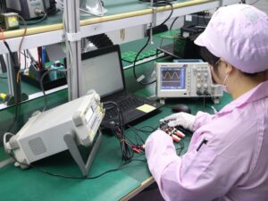
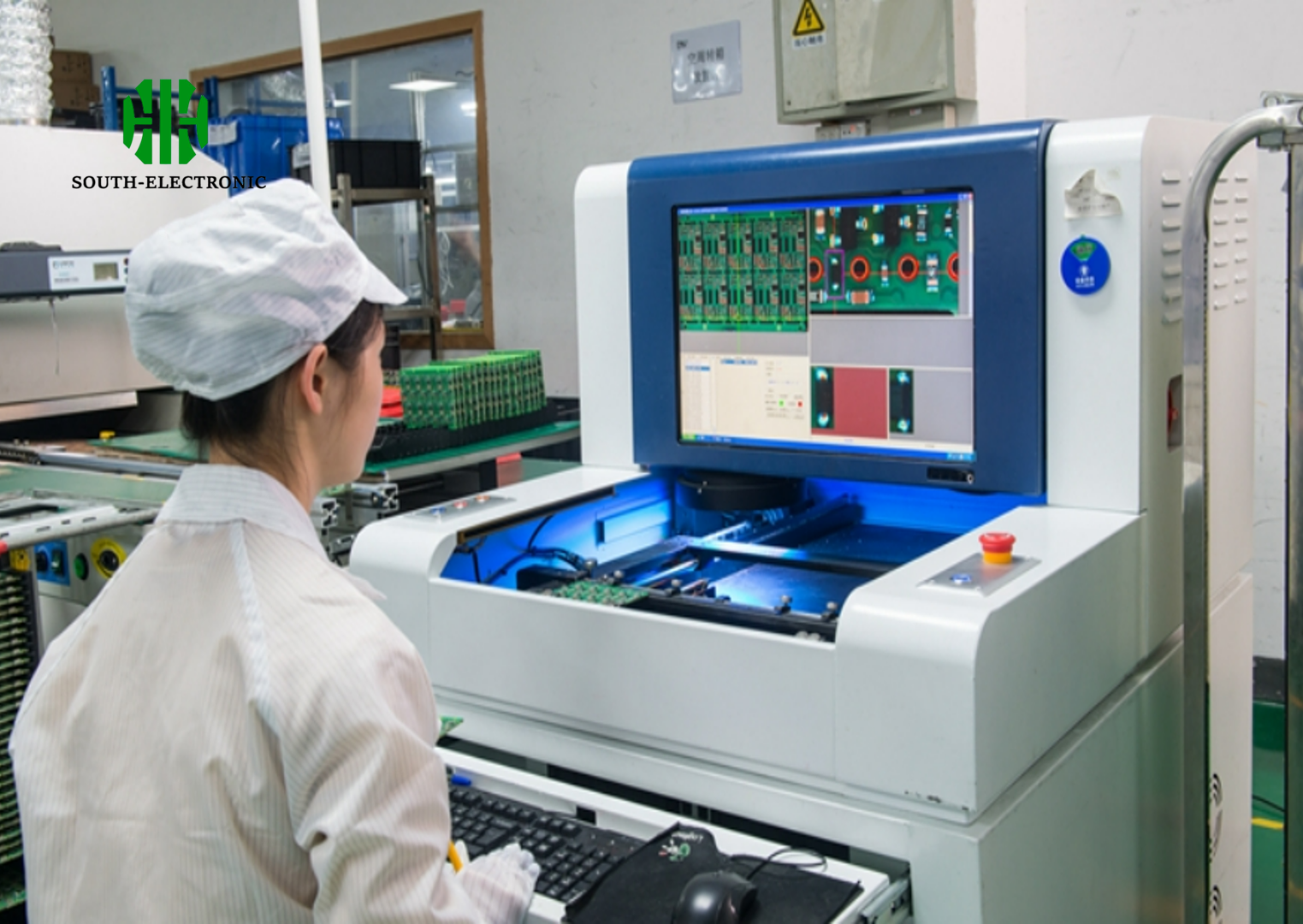
Ensuring high-quality results in SMT assembly is crucial for the performance and reliability of the final product. Several quality control methods are employed throughout the SMT process to detect defects early, prevent assembly issues, and ensure the integrity of the PCB. Two key techniques, Automated Optical Inspection (AOI) and X-ray Inspection, are widely used to maintain high standards in the assembly process. Additionally, adherence to quality certifications such as ISO9001 ensures that all processes are rigorously controlled and meet international standards.
1. Automated Optical Inspection (AOI)
Automated Optical Inspection (AOI) is a non-contact visual inspection method that scans the assembled PCBs to identify any defects such as missing components, misalignments, or soldering issues. AOI machines use high-resolution cameras and pattern recognition software to detect issues at a very early stage of production. The system compares the actual placement and soldering of components against the intended design and layout.
How AOI Ensures Quality:
- Detects Misalignments: AOI quickly identifies any misplaced or skewed components, preventing further issues during the reflow process.
- Checks for Soldering Defects: It examines solder joints to detect common problems such as insufficient solder, solder bridging, or cold solder joints.
- Fast and Accurate: AOI systems offer a fast and highly accurate method for inspecting large volumes of PCBs, which significantly reduces the risk of faulty products reaching the next stage of production.
2. X-ray Inspection
X-ray inspection is particularly useful for inspecting complex PCBs that use advanced components like Ball Grid Arrays (BGAs), where solder joints are hidden beneath the component. Since these joints cannot be visually inspected, X-ray machines allow manufacturers to see inside the PCB and examine the quality of the solder joints and connections.
How X-ray Inspection Ensures Quality:
- Detects Hidden Defects: X-ray inspection reveals issues such as voids in solder joints, cracks, or insufficient solder under BGA and other hidden components.
- Ensures Proper Soldering: It helps ensure that every solder joint is secure and properly formed, even when it can’t be visually inspected.
- Critical for High-Density Designs: As components become smaller and more densely packed, X-ray inspection becomes essential to verify that all connections are functioning properly.
3. ISO9001 Quality Standards
ISO9001 certification is an internationally recognized quality management standard that ensures the company follows a consistent and reliable process in manufacturing. For SMT assembly, adhering to ISO9001 standards means that every step of the process, from design to final assembly, is carefully monitored and controlled.
How ISO9001 Contributes to Quality:
- Process Control: ISO9001 requires that all processes are documented, controlled, and continuously improved, which reduces the likelihood of errors and ensures consistent quality.
- Risk Management: By following ISO9001 standards, manufacturers implement risk management practices that identify potential issues early, leading to fewer defects and a higher rate of successful production.
- Customer Satisfaction: ISO9001 ensures that customer requirements are met, as manufacturers are held to strict quality standards, resulting in reliable products that meet or exceed customer expectations.
Conclusion
Quality control in SMT assembly is achieved through a combination of advanced inspection techniques like AOI and X-ray inspection, as well as adherence to industry-recognized quality standards like ISO9001. These methods ensure that defects are identified and corrected early in the process, reducing the risk of faulty products and ensuring the reliability of the final assemblies. By implementing stringent quality control measures, manufacturers can consistently produce high-performance, defect-free PCBs that meet the highest standards of quality.
Chapter 9
Applications of SMT Assembly in Different Industries
Surface Mount Technology (SMT) assembly has revolutionized the electronics manufacturing industry, making it a key enabler for the production of complex, high-performance, and compact electronic devices across various sectors. SMT assembly is widely used in a broad range of industries due to its ability to support miniaturization, enhance performance, and reduce production costs. In this section, we’ll explore how SMT assembly benefits different industries, along with real-world examples of its application.
1. Consumer Electronics
The consumer electronics industry is perhaps the biggest beneficiary of SMT assembly. With the ever-growing demand for smaller, faster, and more powerful devices, SMT allows manufacturers to produce highly compact circuit boards that support advanced functionality while maintaining affordability.
Applications in Consumer Electronics:
- Smartphones and Tablets: SMT assembly is used to pack hundreds of tiny components onto PCBs in devices like smartphones and tablets. These devices rely on the precision of SMT to integrate processors, memory chips, and communication modules into small, lightweight designs.
- Wearable Devices: From fitness trackers to smartwatches, SMT enables the miniaturization of components, making it possible to create sleek and lightweight wearable technology.
Example: Apple’s iPhones rely heavily on SMT assembly for integrating complex circuits that power everything from the A-series processors to the touchscreen and battery management systems.
2. Automotive Industry
As vehicles become more technologically advanced, the automotive industry is increasingly using SMT assembly to build the complex electronic systems required for modern cars. These systems include everything from infotainment and navigation units to critical safety features like anti-lock braking systems (ABS) and advanced driver assistance systems (ADAS).
Applications in the Automotive Industry:
- Electronic Control Units (ECUs): SMT is used to assemble the highly dense circuit boards in ECUs, which control various functions of the vehicle, such as engine management, braking, and stability control.
- ADAS and Autonomous Driving: Advanced features like lane-keeping assist, adaptive cruise control, and parking sensors rely on SMT to create compact and reliable circuits for sensor processing.
Example: Tesla’s electric vehicles make extensive use of SMT assembly for their ECUs, battery management systems, and self-driving technologies, helping the company reduce the size and weight of critical components.
3. Aerospace and Defense
In the aerospace and defense industries, where reliability, performance, and weight reduction are paramount, SMT assembly is critical for producing advanced electronic systems used in aircraft, satellites, and defense applications. These systems must meet strict performance and durability standards while operating in extreme environments.
Applications in Aerospace and Defense:
- Avionics: SMT assembly is used to create compact and lightweight circuit boards for avionics systems, including communication, navigation, and flight control systems.
- Satellites and Space Exploration: SMT enables the production of lightweight and highly reliable electronics used in satellites and space probes, where space constraints and harsh environmental conditions are key factors.
Example: The Mars Rover, launched by NASA, relies on SMT-assembled circuits to control its navigation, power systems, and scientific instruments, all designed to withstand the extreme conditions of space.
4. Medical Devices
In the medical field, SMT assembly is essential for creating highly precise, reliable, and miniaturized electronics used in diagnostic equipment, monitoring devices, and implantable medical devices. These devices often require strict standards for performance, reliability, and safety.
Applications in Medical Devices:
- Wearable Medical Devices: Devices like heart rate monitors, glucose sensors, and wearable ECG machines rely on SMT assembly for miniaturization and reliability, making them comfortable and easy for patients to use.
- Implantable Devices: Pacemakers and cochlear implants use SMT technology to create compact and efficient circuitry that can be implanted in the human body and operate reliably over extended periods.
Example: Medtronic’s pacemakers and insulin pumps are examples of medical devices that use SMT assembly to create compact, highly reliable systems that are critical for patient health and well-being.
5. Telecommunications
Telecommunications systems, which are responsible for transmitting and processing data at high speeds, benefit significantly from SMT assembly. With the growing demand for faster and more reliable communication, SMT is used to create the densely packed, high-performance PCBs needed for modern networking equipment.
Applications in Telecommunications:
- Cellular Base Stations: SMT is used to build the circuit boards in base stations that handle cellular communication, supporting the expansion of 5G networks.
- Fiber Optic Communications: High-speed data transmission equipment, such as fiber optic transceivers and network switches, uses SMT to assemble compact and efficient circuits that ensure reliable signal transmission.
Example: Cisco’s high-speed routers and networking equipment utilize SMT assembly to meet the high-performance demands of modern telecommunication networks, including 5G and fiber optics.
6. Industrial and Manufacturing Automation
In industrial and manufacturing automation, SMT assembly is critical for producing the control systems that power robots, conveyor systems, and monitoring equipment. These systems must be highly reliable and often operate in harsh environments.
Applications in Industrial Automation:
- Programmable Logic Controllers (PLCs): SMT is used to create the PCBs for PLCs, which control machinery and processes in factories and industrial settings.
- Robotics: SMT-assembled control boards are essential for the precise movements and operations of industrial robots used in automation.
Example: Siemens’ industrial control systems and automation equipment use SMT assembly to create reliable and compact PCBs that manage complex factory processes.
Conclusion
SMT assembly is an essential technology across a wide range of industries, from consumer electronics to aerospace. Its ability to create compact, reliable, and high-performance PCBs has made it the standard for modern electronics manufacturing. Whether it’s enabling the miniaturization of smartphones or ensuring the reliability of aerospace systems, SMT assembly plays a critical role in today’s advanced technological world.
Chapter 10
Choosing the Right SMT Assembly Partner
Selecting the right Surface Mount Technology (SMT) assembly service provider is a critical decision that can significantly impact the quality, cost, and timeline of your project. Whether you are working on small-scale prototypes or high-volume production runs, choosing a partner who aligns with your technical and business needs is essential for ensuring the success of your electronics assembly. Here are some of the key factors to consider when selecting an SMT assembly provider, along with insights on why quality, turnaround time, and technical support are crucial for successful projects.
1. Quality Standards and Certifications
Quality is paramount in SMT assembly, as any defects in the final product can lead to failures in the field, increased costs, and damage to your reputation. Ensuring that your SMT assembly partner adheres to high-quality standards and holds relevant certifications is essential.
Factors to Consider:
- ISO9001 Certification: Look for providers that are ISO9001 certified. This certification demonstrates that the company follows strict quality management standards, ensuring consistent, reliable results in the manufacturing process.
- In-House Quality Control: Ensure the provider has robust quality control processes, such as Automated Optical Inspection (AOI), X-ray inspection, and in-circuit testing, to catch defects early and maintain high standards throughout the assembly process.
- Component Sourcing Quality: Make sure that the provider sources high-quality, reliable components from trusted suppliers to prevent issues such as counterfeit or low-grade parts from entering your supply chain.
Why It Matters: High-quality assembly minimizes defects and rework, resulting in a more reliable product and lower overall costs in the long run.
2. Turnaround Time and Delivery Reliability
For many electronics projects, time-to-market is a critical factor. A reliable SMT assembly partner should be able to meet your project deadlines without compromising quality. Fast turnaround times can give you a competitive edge, especially in rapidly evolving industries like consumer electronics and telecommunications.
Factors to Consider:
- Lead Time: Ask about the provider’s average lead time for both prototype runs and full production orders. Providers with streamlined processes and efficient production lines can offer faster turnaround times.
- On-Time Delivery Track Record: Ensure the provider has a proven track record of delivering projects on time. Delays in the assembly process can have a cascading effect on your entire production schedule.
- Capacity for Scaling: If you expect to scale your production in the future, make sure the partner has the capacity and flexibility to handle larger volumes without significant delays.
Why It Matters: Fast, reliable delivery allows you to bring your products to market quickly, giving you a competitive advantage and helping you meet customer demands on time.
3. Technical Expertise and Support
A competent SMT assembly partner should provide more than just assembly services—they should offer technical expertise and support to help you navigate challenges in design, component selection, and manufacturing. The right partner will be able to offer insights and solutions that can improve the quality and manufacturability of your product.
Factors to Consider:
- Engineering Support: Look for a partner with an experienced engineering team that can review your PCB design and offer suggestions for improvements, such as optimizing for manufacturability (DFM) or minimizing potential assembly issues.
- Prototyping Assistance: For new products, it’s important to work with a provider that can quickly turn around prototypes and offer feedback on potential design flaws or areas for improvement before moving to mass production.
- Post-Sales Support: Technical support doesn’t end once the boards are assembled. Make sure your partner offers post-sales technical assistance to address any issues that arise after delivery.
Why It Matters: Working with an SMT assembly provider that offers strong technical support can help you avoid costly mistakes, ensure smooth production runs, and improve the overall quality of your product.
4. Flexibility and Customization Options
Not all SMT assembly projects are the same, and your assembly partner should offer flexibility to accommodate your unique needs. Whether it’s a low-volume prototype or a high-volume production run, your partner should be able to tailor their services to meet your specific requirements.
Factors to Consider:
- Low-Volume and High-Volume Capability: Ensure that the provider can handle both small prototype runs and larger production batches. Some providers specialize in high-volume runs, while others excel in flexible low-volume production.
- Customization: If your project requires specific materials, components, or processes, make sure the provider can accommodate these custom requests. This is especially important for industries like medical or aerospace, where compliance with strict standards may be required.
- No Minimum Order Requirements: For startups or companies developing prototypes, it’s important to find a partner who is willing to work on small-scale projects without imposing high minimum order quantities.
Why It Matters: Flexibility ensures that you can adapt to changing project requirements and still receive high-quality assembly services tailored to your exact needs.
5. Cost-Effectiveness
While cost should never be the sole deciding factor when choosing an SMT assembly partner, it is important to find a provider who offers competitive pricing without sacrificing quality. Evaluate the overall value offered by the provider, considering factors such as quality, service, and support, rather than focusing solely on the lowest price.
Factors to Consider:
- Transparent Pricing: Ensure that the provider offers transparent pricing with no hidden costs. Request detailed quotes that include all aspects of the assembly process, from component sourcing to testing.
- Cost Optimization: Look for partners who offer cost-saving options, such as bulk discounts for larger orders or suggestions for more affordable component alternatives without compromising quality.
Why It Matters: Competitive pricing helps you stay within your budget, but it’s important to balance cost with the level of quality and support you receive. A cheaper option that results in poor-quality assemblies can lead to more expensive problems down the line.
6. Global Shipping and Logistics
If you operate in different countries or regions, consider an SMT assembly partner with global shipping capabilities and a proven logistics network. The ability to reliably ship products to various locations while managing customs and other international logistics issues is crucial for companies operating on a global scale.
Factors to Consider:
- Global Reach: Ensure the partner can ship internationally and has experience dealing with customs regulations, tariffs, and duties in your target markets.
- Packaging and Handling: The provider should offer proper packaging to protect sensitive PCBs during shipping, as well as reliable tracking systems to keep you informed throughout the delivery process.
Why It Matters: Efficient shipping and logistics management help avoid delays, reduce damage risks, and ensure that your products reach their destinations on time.
Conclusion
When choosing the right SMT assembly partner, it’s essential to evaluate key factors such as quality standards, turnaround time, technical support, flexibility, and cost-effectiveness. Ensuring that your partner can meet your specific requirements and deliver reliable, high-quality results will make a significant difference in the success of your project. Prioritizing these factors ensures a smooth manufacturing process, faster time to market, and a final product that meets the highest standards of quality and performance.
Get in touch
Where Are We?
Industrial Park, No. 438 Donghuan Road, No. 438, Shajing Donghuan Road, Bao'an District, Shenzhen, Guangdong, China
Floor 4, Zhihui Creative Building, No.2005 Xihuan Road, Shajing, Baoan District, Shenzhen, China
ROOM A1-13,FLOOR 3,YEE LIM INDUSTRIAL CENTRE 2-28 KWAI LOK STREET, KWAI CHUNG HK
service@southelectronicpcb.com
Phone : +86 400 878 3488
Send us a message
The more detailed you fill out, the faster we can move to the next step.


