
Have you ever wondered why your high-speed IoT device glitches unexpectedly? A smartphone screen flickers during video calls? Signal integrity holds the answers.
Signal integrity[^1] ensures electrical signals maintain their quality from transmitter to receiver in circuits. It prevents distortions caused by noise, timing errors, or physical interference – especially critical in 5G and IoT devices where data accuracy determines success or failure.
)
Think this only concerns engineers? Every tech user faces its outcomes daily. Let’s break down why signals get "corrupted" and how to prevent costly design errors.
Key Elements of Signal Integrity
Why do signals deteriorate even in carefully designed circuits? Three silent saboteurs wait to scramble your data.
Core signal integrity elements include timing accuracy[^2], voltage level consistency[^3], and waveform purity. These determine whether a digital ‘1’ stays a ‘1’ – not a deformed ‘0’ – across transmission lines.
)
The Invisible Threats Matrix
| Threat | Cause | Visible Impact | Detection Tool |
|---|---|---|---|
| Signal Noise | EMI from adjacent circuits | Random data errors | Spectrum analyzer |
| Timing Jitter | Clock signal instability | Video/audio desync | Eye diagram analysis |
| Crosstalk | Parallel trace coupling | Ghost data packets | 3D field solver simulations |
| Impedance Shift | Dielectric material variance | Signal reflections at connectors | Time-domain reflectometer |
I once spent 72 hours debugging a USB 3.0 interface that failed at 5 Gbps speeds. TDR measurements revealed a 2mm impedance discontinuity in a connector – proof that microscopic flaws create system-level failures.
Basic Principles to Preserve Signal Integrity
Can you avoid signal chaos without PhD-level expertise? Master four defense strategies.
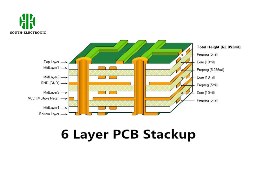
Preserve signal integrity through controlled impedance routing[^4], optimized stack-up design, proper termination techniques[^5], and electromagnetic shielding. These form the foundation of reliable high-speed PCB layouts.
)
The Prevention Toolkit
1. Impedance Control
- Use microstrip/stripline calculators for trace width/spacing
- Maintain ±10% tolerance from source to load
- Example: 50Ω USB differential pairs require 0.15mm traces on FR4
2. Routing Discipline
- Avoid 90° angles (use 45° or curved traces)
- Length-match critical buses (DDR, PCIe)
- Separate analog/digital grounds with moats
3. Terminator Types
| Termination | Best For | Power Draw | Complexity |
|---|---|---|---|
| Series | Clock signals | Low | Medium |
| Parallel | Memory interfaces | High | Simple |
| AC | High-frequency lines | Moderate | Advanced |
During a smartwatch design, adding 22Ω series resistors to MIPI display lines eliminated screen flickering – a $0.02 fix saving $20,000 in recalls.
How to Avoid Common Signal Integrity Mistakes in High-Speed Designs?
Why do 68% of high-speed designs fail first prototypes? Hidden landmines in everyday decisions.
Avoid signal integrity pitfalls[^6] by preventing split planes under critical traces, mismatched via structures, inadequate power filtering, and oversights in material frequency response – all proven failure accelerators.
)
The 5 Costly Errors Checklist
Error 1: "This 10-layer board can handle 25 Gbps…"
Reality: Standard FR4 struggles beyond 5 GHz. Switch to Rogers 4350B for mmWave designs.
Error 2: "Decoupling capacitors? More must be better!"
Truth: Poor capacitor placement creates resonant peaks. Follow the 0.1μF per power pin rule.
Error 3: "Our 1mm via is industry standard"
Danger: Via stubs act as antennas. Use back-drilling or blind vias for >10 Gbps signals.
Error 4: "Ground planes are all the same"
Fact: A 3.5μm copper roughness increases insertion loss by 18% at 10 GHz. Specify low-profile foils.
Error 5: "Simulation matches lab results…"
Watch: Component parasitics (QFN vs. BGA packages) alter real-world performance by up to 40%.
After a failed HDMI 2.1 prototype, we discovered 8mil differential pair spacing (instead of 6mil) caused 30% eye diagram closure. Precision trumps assumptions.
Conclusion
Mastering signal integrity transforms erratic prototypes into reliable devices. Control impedance, eliminate noise paths, validate simulations – your circuits will speak clearly.
[^1]: Understanding signal integrity is crucial for anyone working with electronic devices, as it directly affects performance and reliability.
[^2]: Timing accuracy is a key factor in ensuring data integrity in circuits; exploring this can enhance your knowledge of electronic design.
[^3]: Voltage level consistency is vital for maintaining signal quality; learning more can help prevent costly errors in circuit design.
[^4]: Controlled impedance routing is vital for high-speed performance. Discover its impact and best practices in this informative link.
[^5]: Different termination techniques can significantly affect circuit performance. Learn about them to enhance your designs.
[^6]: Understanding these pitfalls can help you avoid costly mistakes in your designs, ensuring better performance and reliability.

