
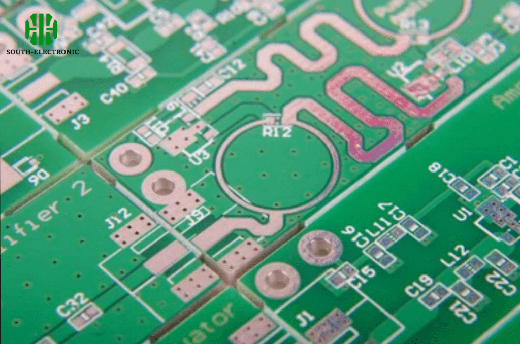
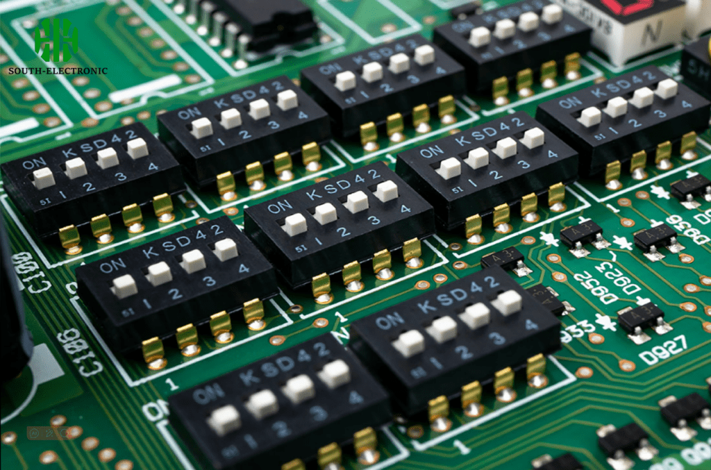
Ever struggled to identify components on a crowded PCB? Silkscreen markings and soldermask layers are critical yet misunderstood elements. Let me break down these two pillars of circuit board functionality.
Silkscreen[^1] applies visible labels for component placement, while soldermask creates an insulating protective layer. Silkscreen aids assembly, soldermask[^2] prevents short circuits – both essential for reliable PCB operation[^3].
Understanding these layers is just the beginning. Let’s dissect their unique roles through four key questions every designer should ask.
What Is Silkscreen On a PCB?
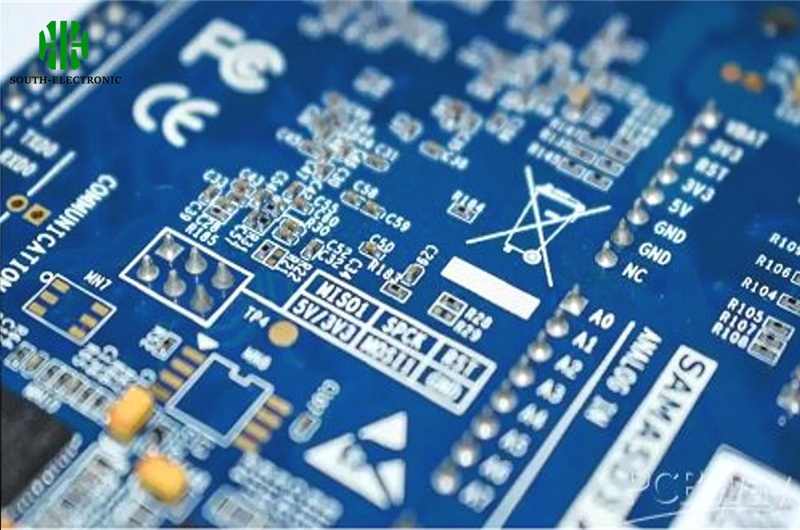
Can’t read component designators? That’s where silkscreen shines. This top-layer ink marking system acts as your PCB’s instruction manual.
Silkscreen is the white (usually) printed layer showing component outlines, logos, and test points. It uses epoxy ink applied through screen printing or modern inkjet methods for precise labeling.
Beyond Basic Labeling
Three critical aspects define modern silkscreen application:
-
Resolution Requirements
Feature Minimum Line Width Character Height Manual Assembly 0.2mm 1.5mm Automated Lines 0.15mm 1.0mm -
Material Choices
- Standard epoxy ink (most common)
- Liquid photo-imageable (LPI) for finer details
- UV-curable inks for quick processing
-
Alignment Challenges
Registration marks ensure multi-layer alignment. New thermal cure methods reduce positional drift compared to traditional air-drying techniques. I once ruined a batch by skipping registration checks – learn from my mistake!
Is Overlay the Same as Silkscreen?
Heard "overlay" in manufacturing discussions? Terminology confusion can lead to production errors.
While some manufacturers use "overlay" interchangeably with silkscreen, technically overlay refers to protective film layers. True silkscreen specifically denotes component labeling ink.
)
Terminology Breakdown
Clear definitions prevent misunderstandings:
-
Technical Definitions
- Silkscreen: Permanent ink markings
- Overlay: Polyimide films in flexible circuits
-
Industry Usage Survey
Region Preferred Term North America Silkscreen (85%) Europe Overlay (60%) Asia Legend (70%) -
Design Implications
When specifying "silkscreen" in Gerber files, always include:- Color specifications
- Font type/size
- Layer position markers
Can You Remove Silkscreen from PCB?
Accidental silkscreen errors happen. Can you fix them? The answer depends on materials and methods.
Yes, silkscreen can be removed using solvents or mechanical abrasion. However, removal risks damaging underlying soldermask and requires professional equipment for clean results.
)
Removal Process Breakdown
Three removal scenarios with different approaches:
-
Spot Corrections
- Use acetone-soaked swabs (epoxy inks only)
- Maximum 3-second contact time
- Follow with IPA rinse
-
Full-Layer Removal
Method Success Rate Risk Level Chemical Bath 95% High Laser Ablation 98% Medium Manual Scraping 80% Very High -
Post-Removal Considerations
- Check soldermask integrity
- Verify copper trace exposure
- Apply new silkscreen within 24hrs
How to Make Silkscreen PCB?
Creating professional silkscreen starts with proper design practice. Follow these steps to avoid common pitfalls.
Design silkscreen in CAD software[^4] using dedicated layers, choose appropriate line widths, and coordinate with your manufacturer’s capabilities. Always perform test prints before full production.
Production Workflow
Five-stage process for reliable results:
-
Design Phase
- Use vector fonts (avoid TrueType)
- Minimum 0.15mm line width
- 0.3mm clearance from pads
-
Artwork Preparation
Output Format Resolution Film Gerber RS-274X 20,000 DPI Direct PDF Vector 600 DPI -
Printing Methods Comparison
Method Accuracy Cost Speed Screen ±0.1mm $ Medium Inkjet ±0.05mm $$ Fast LPI ±0.03mm $$$ Slow -
Curing Process
- Standard: 30mins @ 150°C
- Fast-cure: 5mins @ 180°C (requires special inks)
-
Quality Control
- 3-point optical inspection
- Adhesion tape test
- Humidity resistance check
Conclusion
Silkscreen guides assembly, soldermask protects circuitry – master both for robust PCBs. Always clarify terminology with manufacturers and test designs rigorously before full-scale production.
[^1]: Explore this link to understand how silkscreen enhances PCB design and assembly, ensuring accurate component placement and functionality.
[^2]: Discover the importance of soldermask in preventing short circuits and protecting your PCB, a crucial aspect for reliable electronics.
[^3]: Learn how these two layers contribute to the overall performance and reliability of PCBs, essential for any electronics designer.
[^4]: Discover top CAD software options that can streamline your PCB design process and improve your silkscreen results.

