
Custom Single Layer PCB Manufacturing Services
Min trace 3/3 mil | OSP / HASL | FR-4 & High-TG | AOI & E-Test
We manufacture high-precision single-layer PCBs for a wide range of applications including consumer electronics, automotive, and telecommunications. Our rigorous production standards ensure stable quality and consistent performance for both prototyping and large-scale production.
Single Layer PCB Capabilities
Single Layer PCB Process Capability
-
Layer Count
1 layer
-
PCB Dimensions
≤24*48inch(610*1220mm)
-
Materials Types
FR-4 | High Tg | Halogen-free | Flexible materials | Metal substrate material
-
Material Brand
Lianmao|Shengyi| Taiyao| Nanya, Panasonic|Isola|Nelco|Rogers|Taconic|Arlon...
-
Board Thickness
0.2 mm - 3.2 mm
-
Finish Treatment
OSP | Lead-free HASL | Immersion Tin | Immersion Silver | Thick Gold Plating | Silver Plating
-
Copper thickness
0.5 OZ - 4 OZ
-
SolderMask Color
Green| Blue| Black|Yellow| Red|Purple| White...
-
Finish Treatment
OSP | Lead-free HASL | Immersion Tin | Immersion Silver | Thick Gold Plating | Silver Plating
Why Choose Us for Single Layer PCB Manufacturing
We support engineers with reliable single-layer PCB manufacturing,
from prototype builds to stable repeat production.
Every single-layer PCB is thoroughly reviewed by our engineers to ensure manufacturability, material selection, and assembly compatibility before production.
We prioritize consistent quality across batches, providing dependable support for both prototypes and long-term manufacturing needs.
Experienced in handling various applications, we can accommodate tight tolerances and specific material requirements for diverse industries.
We ensure clear technical communication and prompt responses to effectively support overseas engineering and purchasing teams.
Related Project We Had Done
Single Layer PCB for Consumer Electronics
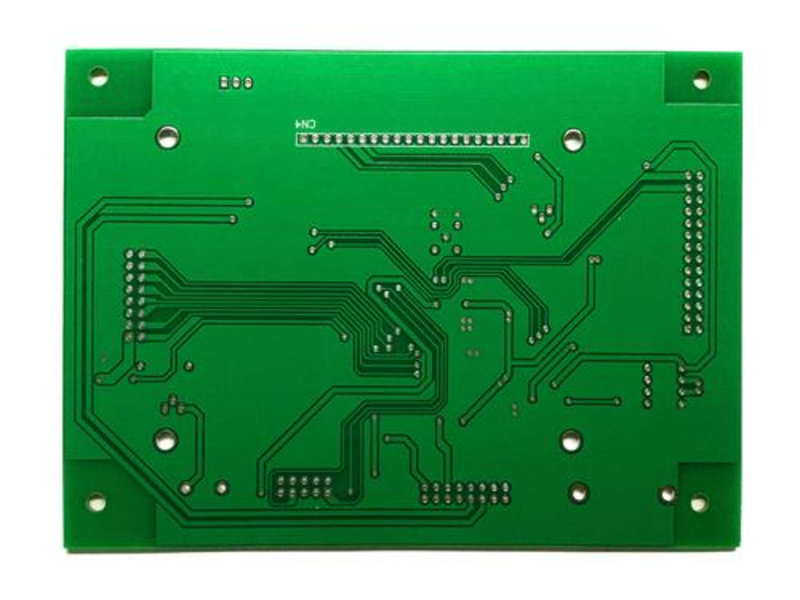
Application
Consumer Electronics
Key Specs
Single-layer, standard FR-4
Challenge
Compact design with low-cost production
Result
High reliability and cost-effective manufacturing for mass production
Single Layer PCB for Automotive Lighting
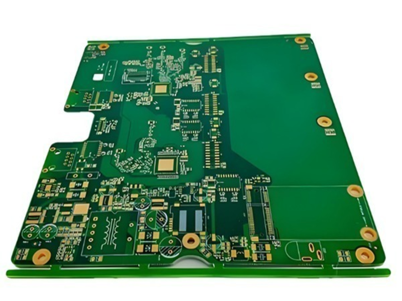
Application
Automotive Lighting Systems
Key Specs
Single-layer, high-temperature materials
Challenge
Durability under extreme conditions and thermal management
Result
Consistent performance and compliance with automotive standards
Single Layer PCB for Telecommunication
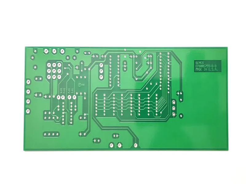
Application
Telecommunication Devices
Key Specs
Single-layer, impedance controlled
Challenge
Support for high-speed data transmission and signal integrity
Result
Stable signal performance and reliable quality throughout production batches
Quality Control & Certifications for Single Layer PCB Production
Common Questions
Most Popular Questions
What is the typical lead time for Single Layer PCB production?
Prototype lead time is typically 7–10 working days.
Mass production lead time depends on quantity and specifications.
Can you accommodate custom specifications?
Yes, we can customize specifications such asmaterial type, thickness, and surface finish.
Is there a minimum order quantity?
No, we provide solutions with no minimum order quantity for flexibility.
What surface finishes are available?
Options include OSP, HASL, and ENIG.
What files are required to get an single-layer PCB quotation?
Please provide Gerber files, PCB quantity, and any special requirements such as impedance control or material preference.
Send Us a Message
The more detailed you fill out, the faster we can move to the next step.
