

Holding your phone’s 5G connection while moving? That flawless signal relies on hidden PCB superheroes – SMA connectors. Let’s decode what makes them mission-critical for modern electronics.
Holding your phone’s 5G connection while moving? That flawless signal relies on hidden PCB superheroes – SMA connectors[^1]. Let’s decode what makes them mission-critical for modern electronics.
SMA (SubMiniature version A) connectors are coaxial RF interfaces maintaining signal integrity[^2] up to 18 GHz in PCBs. Their threaded coupling and 50-ohm impedance[^3] prevent signal loss, making them essential for 5G, radar systems, and satellite communications requiring precise high-frequency connections.
While SMA’s significance is clear, their real magic lies in smart engineering decisions. We’ll explore their structural DNA, performance advantages, variants, and installation best practices to help you leverage their full potential.
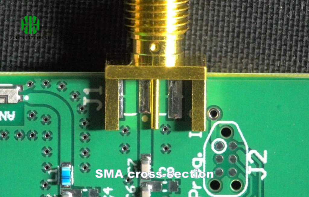
How Is SMA Structurally Designed for PCBs?
Ever wonder how something smaller than a dime handles 18 GHz signals? SMA’s mechanical blueprint reveals a fortress-like architecture protecting delicate RF pathways.
SMA connectors use concentric metal shells with air-tight threaded coupling, PTFE dielectric insulation, and precision-machined center contacts to create stable 50Ω impedance paths. This military-grade construction minimizes insertion loss (<0.1dB) while withstanding vibration and temperature extremes (-65°C to +165°C).
)
Three-Layered Defense Mechanism
SMA's effectiveness stems from calculated layer interactions:
| Layer | Function | Material Used | Critical Specs |
|---|---|---|---|
| Outer Shell | EMI shielding & mechanical support | Stainless steel/beryllium copper | 0.5μm gold plating |
| Dielectric | Signal insulation | PTFE (Teflon) | εᵣ=2.1, loss tangent 0.0003 |
| Center Conductor | Signal transmission | Gold-plated brass | 0.9mm diameter ±0.01mm |
The threaded coupling (5/8-24 UNEF thread) ensures 360° shielding – crucial for GHz-range signals where even 0.1mm gaps cause reflections. PTFE's stable dielectric constant across temperature changes prevents impedance drifting.
Why Are SMA Connectors Ideal for High-Frequency PCB Applications?
When your Wi-Fi router drops signal at 6 GHz, SMA stands guard. Their high-frequency prowess comes from physics-first engineering.
SMA's 50Ω impedance matches PCB transmission lines, preventing signal reflections up to 18 GHz. The hermetic interface maintains VSWR <1.3:1 even after 500 mating cycles, outperforming most RF connectors in sustained high-frequency stability.
)
Battling High-Frequency Demons
Five key factors make SMA exceptional:
-
Skin Effect Management
Gold plating (3-50μ") on contacts reduces surface resistivity to 2.44μΩ·cm, crucial as GHz signals travel along conductor surfaces. -
Dielectric Loss Control
PTFE's ultra-low loss tangent (0.0003 vs. 0.02 for standard FR4) cuts energy absorption by 98% at 10 GHz. -
Mode Suppression
The λ/4 choke design in SMA jacks suppresses higher-order modes above 18 GHz, keeping signals clean. -
Thermal Compensation
The stainless steel-PTFE composite structure expands/contracts uniformly across -65°C to +165°C, maintaining <0.05mm dimensional stability. -
Shielding Effectiveness
Triple-point contact design[^4] achieves 120dB shielding at 10 GHz – vital for crowded RF environments.
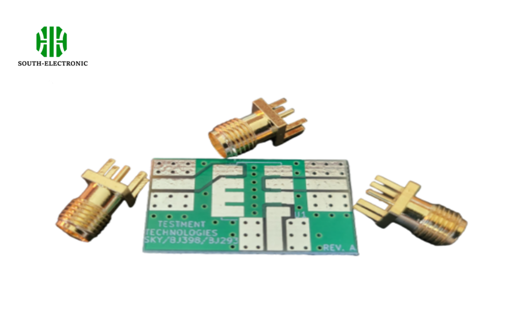
What Types of SMA PCB Connectors Exist and How Do They Differ?
Not all SMAs are created equal. The 3 main species serve distinct PCB ecosystems – choose wrong, and your signals suffer.
Key SMA variants include PCB Edge Mount (direct soldering, 0-12 GHz), Surface Mount (automated assembly, 0-18 GHz), and Through-Hole (high mechanical stress, 0-6 GHz). Material grades (commercial vs. military) further differentiate performance specs.
)
SMA Selection Matrix
Critical differentiators across types:
| Parameter | Edge Mount | Surface Mount | Through-Hole |
|---|---|---|---|
| Max Frequency | 12 GHz | 18 GHz | 6 GHz |
| PCB Real Estate | 8.5mm edge space | 6x6mm land pattern | 10mm drill area |
| Assembly Method | Manual soldering | Reflow compatible | Wave soldering |
| Vibration | Fair | Excellent | Good |
| Cost Factor | $1.2-$3.5 | $0.8-$2.1 | $0.5-$1.8 |
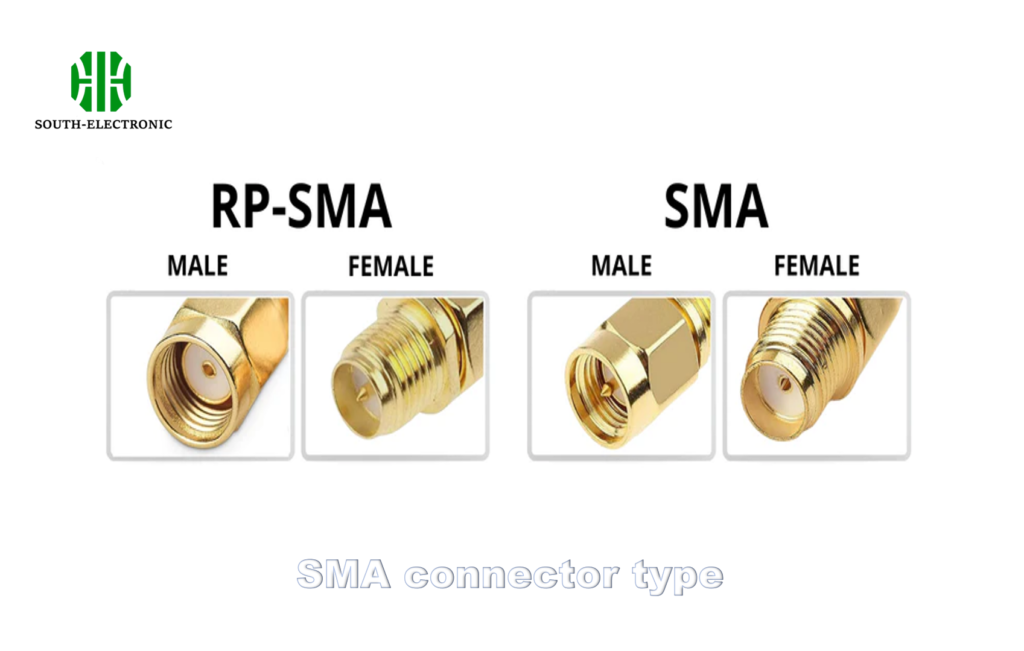
Military-spec (MIL-STD-348) variants add passivation layers and extended temperature ranges (-85°C to +200°C), while reverse-polarity (RP-SMA) swaps gender roles for specific WiFi/BT applications.
What Are the Key Advantages of Using SMA Connectors Over Other RF Interfaces?
In the RF connector showdown, SMA fights dirty – with physics. Its technical superiority often outweighs cost considerations.
Compared to BNC/U.FL alternatives, SMA offers 3x higher frequency range, 10x better shielding, and 50% lower insertion loss. Gold-plated brass contacts ensure 10,000+ mating cycles versus BNC's 500 cycles average.
)
The RF Interface Face-off
| Metric | SMA | BNC | U.FL |
|---|---|---|---|
| Max Frequency[^5] | 18 GHz | 4 GHz | 6 GHz |
| Insertion Loss[^6] | 0.05dB @6GHz | 0.3dB @4GHz | 0.1dB @3GHz |
| Mating Cycles | 10,000 | 500 | 30 |
| VSWR | 1.3:1 | 1.8:1 | 1.5:1 |
| Shield (dB) | 120 | 90 | 60 |
| Temp Range | -65°C ~+165°C | -40°C ~+85°C | -40°C ~+85°C |
How to Select and Install SMA Connectors for Optimal PCB Performance?
Installing SMA connectors? It’s microsurgery – one wrong move sacrifices GHz performance. Master these selection and soldering protocols[^7].
Select SMA connectors based on 3 factors: Frequency needs (6/12/18 GHz grades), PCB stackup (dielectric constant matching), and mechanical stress. Install using <350°C soldering with <2sec dwell time to prevent PTFE degradation.**
)
Installation Protocol Checklist
-
Footprint Design
- Keep antipads 2x connector diameter (min 5mm clearance)
- Impedance-controlled traces (50Ω ±10%)
- Use grounded coplanar waveguides above 6 GHz
-
Soldering Parameter Lead-Free SAC305 SnPb Peak Temp 245°C ±5°C 215°C ±5°C Preheat 150°C-180°C 120°C-150°C Dwell Time ≤ 2 seconds ≤ 3 seconds -
Post-Assembly
- Measure VSWR[^8] with 3.5mm calibration kit
- Torque to 8 in-lb using SMA-compatible wrench
- Apply silicone conformal coating only to non-mating surfaces
Avoid "SMA disease" – overtightening beyond 12 in-lb deforms threads, increasing VSWR by 0.5:1 per 2 in-lb excess torque.
Conclusion
SMA connectors enable GHz performance through precision engineering – master their selection, installation, and maintenance to unlock reliable high-frequency PCB operation in 5G and aerospace systems.
[^1]: Understanding SMA connectors is crucial for anyone involved in electronics, especially in high-frequency applications like 5G and radar systems.
[^2]: Exploring signal integrity will enhance your knowledge of maintaining high-quality communications in modern electronics, vital for 5G and beyond.
[^3]: Learning about 50-ohm impedance is essential for designing effective RF systems, ensuring optimal performance in various applications.
[^4]: Learn about the importance of shielding effectiveness in RF environments and how this design achieves it.
[^5]: Understanding Max Frequency is crucial for selecting the right RF connector for your application, ensuring optimal performance and reliability.
[^6]: Learn about Insertion Loss to make informed decisions on RF connectors, as it directly affects signal quality and system performance.
[^7]: This link will provide you with essential soldering protocols to ensure high-frequency performance and reliability in your PCB assemblies.
[^8]: Learn about VSWR measurement techniques to ensure your SMA connector installations meet performance standards and avoid signal loss.

