

Understanding the solder paste reflow process
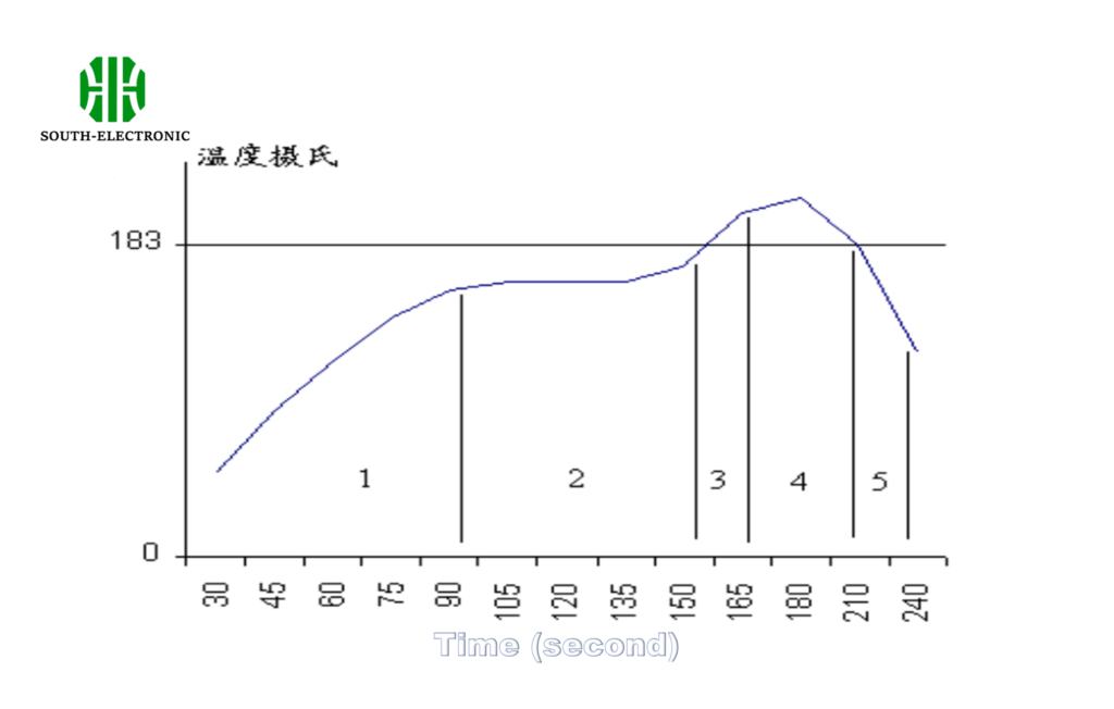
When the solder paste is placed in a heated environment, the solder paste reflow is divided into five stages
- First, the solvent used to achieve the required viscosity and screen printing performance begins to evaporate. The temperature rise must be slow (about 3°C
per second) to limit boiling and splashing, prevent the formation of small solder beads, and some components are sensitive to internal stress. If the external temperature of the component rises too quickly, it will cause fracture. - The flux is active and the chemical cleaning action begins. The same cleaning action occurs in both water-soluble flux and no-clean flux, but at slightly different temperatures. Metal oxides and certain contaminants are removed from the metal and solder particles that are about to be combined. Good metallurgical solder joints require a ‘clean’ surface.
- As the temperature continues to rise, the solder particles first melt individually and begin the "lamp wick" process of liquefaction and surface tin absorption. This covers all possible surfaces and begins to form solder joints.
- This stage is the most important. When all individual solder particles are melted, they combine together to form liquid tin. At this time, surface tension begins to form the solder foot surface: If the gap between the component pin and the PCB pad exceeds 4mil, it is very likely that the pin and the pad will be separated due to surface tension, causing the solder joint to open.
- In the cooling stage, if the cooling is fast, the solder joint strength will be slightly greater, but it cannot be too fast to cause temperature stress inside the component.
Summary of reflow soldering requirements:
It is important to have sufficient slow heating to safely evaporate the solvent, prevent the formation of solder beads and limit the internal stress of the component caused by temperature expansion, which causes fracture reliability problems. Secondly, the flux active stage must have appropriate time and temperature, allowing the cleaning stage to be completed when the solder particles just begin to melt.
The solder melting stage in the time-temperature curve is the most important. It is necessary to fully allow the solder particles to melt completely, liquefy to form metallurgical welding, and evaporate the remaining solvent and flux residue to form the solder foot surface. If this stage is too hot or too long, it may cause damage to the components and PCB. The setting of the solder paste reflow temperature curve is best carried out according to the data provided by the solder paste supplier, and at the same time grasp the principle of temperature stress change inside the component, that is, the heating temperature rise rate is less than 3°C per second, and the cooling temperature drop rate is less than 5°C.
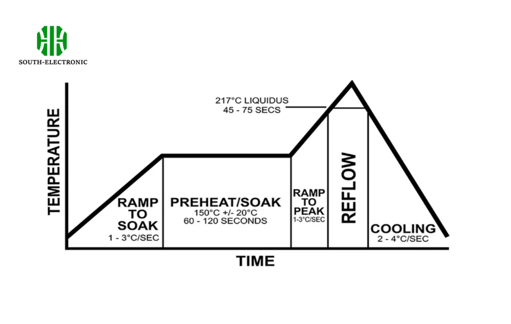
How to set the solder paste reflow temperature profile?
The ideal profile consists of four parts or zones, with the first three zones heated and the last zone cooled. The more temperature zones the furnace has, the more accurate and close the profile can be. Most solder pastes can be successfully reflowed using the four basic temperature zones.
-
Preheating zone, also called ramp zone, is used to raise the temperature of the PCB from the ambient temperature to the required activation temperature. In this zone, the temperature of the product rises continuously at a rate of no more than 2~5°C per second. If the temperature rises too fast, it will cause certain defects, such as fine cracks in ceramic capacitors, while if the temperature rises too slowly, the solder paste will overheat and not have enough time for the PCB to reach the activation temperature. The preheating zone of the furnace generally accounts for 25~33% of the total length of the heating channel.
-
Active zone, sometimes called dry or soaking zone, this zone generally accounts for 33-50% of the heating channel and has two functions. The first is to sense the temperature of the PCB at a fairly stable temperature, allowing components of different masses to be homogenous in temperature and reduce their relative temperature difference. The second function is to allow the flux to be activated and volatile substances to evaporate from the solder paste. The general active temperature range is 120~150°C
-
Reflow zone, sometimes called peak zone or final heating zone. The function of this zone is to increase the temperature of the PCB assembly from the active temperature to the recommended peak temperature. The active temperature is always a little lower than the melting point of the alloy, and the peak temperature is always at the melting point. The typical peak temperature range is 205~230°C. If the temperature setting of this zone is too high, the temperature rise slope will exceed 2~5°0 per second or the reflow peak temperature will be higher than the recommended one. This situation may cause excessive curling, delamination or burning of the PCB and damage the integrity of the component
-
The ideal cooling zone curve should be a mirror image of the reflow zone curve. The closer to this mirror image relationship, the tighter the solid structure of the solder joint, the higher the quality of the solder joint, and the better the bonding integrity.
The first parameter to consider when making a temperature curve is the speed setting of the conveyor belt, which will determine the time the PCB spends in the heating channel. Typical solder paste manufacturing plant parameters require a 3-4 minute heating curve. The total heating channel length divided by the total heating temperature sensing time is the accurate conveyor belt speed. For example, when the solder paste requires a four-minute heating time, a six-foot heating channel length is used, and the calculation is: 6 feet ÷ 4 minutes = 1.5 feet per minute = 18 inches per minute.
Next, the temperature setting for each zone must be determined. It is important to understand that the actual zone temperature is not necessarily the displayed temperature of the zone. The displayed temperature only represents the temperature of the thermistor in the zone. If the thermocouple is closer to the heating source, the displayed temperature will be higher than the zone temperature. The closer the thermocouple is to the direct channel of the PCB, the more the displayed temperature will reflect the zone temperature.
Reflow Profiles That Benefit from Ramp-to-Reflow
Many older ovens tend to heat different parts of an assembly at different rates, depending on the color and texture of the parts and circuit board layers being reflowed. Some areas of an assembly can reach much higher temperatures than others, and this temperature variation is called the DT of the assembly. If the DT is large, some areas of the assembly may receive too much heat, while other areas may not receive enough. This can cause a number of soldering defects, including solder balls, non-wetting, damaged components, voids, and burnt residues.
Why and When to Soak?
The sole purpose of the soak zone is to reduce or eliminate large DTs. The soak should equalize the temperature of all parts in the assembly before the assembly reaches the solder reflow temperature so that all parts reflow at the same time. Since a soak zone is not necessary, the profile can be changed to a linear ramp-to-reflow (RTS) reflow profile.
It should be noted that a soak zone is generally not necessary to activate the flux chemistry in the solder paste. This is a common misconception in the industry that should be corrected. Most solder paste chemistries show adequate wetting activity when a linear RTS profile is used. In fact, wetting is generally improved using an RTS profile.
| Stage | Zone Temperature Setting | Actual Board Temp at End of Zone |
|---|---|---|
| Preheating | 210°C (410°F) | 140°C (284°F) |
| Soak | 177°C (350°F) | 150°C (302°F) |
| Reflow | 250°C (482°F) | 210°C (410°F) |
Ramp-Soak-Reflow Profile
The Ramp-Soak-Reflow (RSS) profile can be used with RMA or no-clean chemistries, but is generally not recommended for water-based chemistries because the RSS soak zone may prematurely destroy the solder paste activator, resulting in inadequate wetting. The only purpose of using an RSS profile is to eliminate or reduce DT.
The RSS profile starts with a steep ramp, 10°C, with a maximum rate of 2-3°C over a target time of approximately 150°C over a 90 second target time. Subsequently, the assembly is held at 150°C to 170°C for 90 seconds; the assembly should reach temperature equilibrium at the end of the holding zone. After the holding zone, the assembly enters the reflow zone and reflows at 183°C for 60 (± 15) seconds.
The entire temperature profile should last from 45°C to a peak temperature of 215 (+ 5)°C for 3.5 to 4 minutes. The cooling rate should be controlled at 4°C per second. Generally, faster cooling rates can produce finer grain structure and higher strength and brighter solder joints. However, exceeding 49°C per second will cause temperature shock.
Heating-Reflow
The RTS temperature profile can be used for any chemical composition or alloy and is preferred for water-soluble solder paste and difficult-to-solder alloys and parts. The RTS temperature profile has several advantages over the RSS. RTS generally produces brighter solder joints and fewer solderability problems because the solder paste reflowed under the RTS temperature profile retains its flux carrier during the preheat stage. This will also improve wettability better, so RTS should be used for alloys and parts that are difficult to wet.
Because the temperature ramp rate of the RTS curve is so controlled, there is less chance of soldering defects or temperature shock. In addition, the RTS curve is more economical because the heating energy in the front half of the furnace is reduced. In addition, troubleshooting RTS is relatively simple, and operators who have experience in troubleshooting RTS curves should have no difficulty adjusting the RTS curve to achieve the optimal temperature curve effect.
Setting the RTS Temperature Curve
The RTS curve is simply a temperature ramp from room temperature to the peak reflow temperature. The RTS curve temperature ramp zone acts as a preheating zone for the assembly, where the flux is activated, volatiles are volatilized, the assembly is ready for reflow, and temperature shock is prevented. The typical temperature ramp rate of the RTS curve is 0.6~1.8°C per second. The first 90 seconds of the temperature ramp should be as linear as possible.
The basic rule of temperature ramp for the RTS curve is that two-thirds of the curve is below 150°C. After this temperature, the active system in most solder pastes begins to fail quickly. Therefore, keeping the front end of the curve cooler will keep the active agent longer, resulting in good wetness and bright solder joints.
The reflow zone of the RTS curve is the stage where the assembly reaches the solder reflow temperature. After reaching 150°C, the peak temperature should be reached as quickly as possible and the peak temperature should be controlled at 215(+5)°C with a liquefaction residence time of 60(± 15) seconds. This time above liquefaction will reduce flux entrapment and voiding and increase tensile strength. Like RSS, the RTS curve length should also be a maximum of 3.5~4 minutes from room temperature to peak temperature, with a cooling rate controlled at 4°C per second
Troubleshooting RTS curves
The principles for troubleshooting RSS and RTS curves are the same: adjust the temperature and time of the curve as needed to achieve the optimal result. Often this requires trial and error, slightly increasing or decreasing the temperature and observing the results. The following are common reflow problems encountered using the RTS curve, and how to solve them.
-
Solder Balling: Many small solder balls are trapped around the perimeter of the flux residue after reflow. On the RTS curve, this is usually the result of a ramp rate that is too slow, as the flux carrier burns out before reflow and metal oxidation occurs. This problem can usually be solved by slightly increasing the ramp rate of the curve. Solder balls can also be the result of a ramp rate that is too fast, but this is less likely with the RTS curve because of its relatively slow, more even ramp.
-
Solder Beading: Often confused with solder balls, solder beads are one or more large balls of solder that usually land around chip capacitors and resistors. Although this is often the result of excessive solder paste buildup during screen printing, it can sometimes be solved by adjusting the temperature curve. Like solder balls, solder beads produced on an RTS curve are usually the result of a ramp rate that is too slow. In this case, the slow ramp rate causes capillary action, drawing unreflowed solder paste from the solder accumulation to the underside of the component. During reflow, this solder paste forms solder beads and is squeezed out to the side of the component due to the surface tension of the solder pulling the component to the board. As with solder balls, the solution to solder beads is to increase the ramp rate until the problem is solved.
-
Poor wetting: Poor wetting is often the result of the time-to-temperature ratio. The activator in the solder paste is composed of organic acids, which degrade with time and temperature. If the curve is too long, the wetting of the solder joint may be impaired. Because the solder paste activator is usually maintained for a longer time using the RTS curve, poor wetting is less likely to occur than with RSS. If poor wetting is still observed with RTS, steps should be taken to ensure that the first two-thirds of the curve occurs below 1509C. This will extend the life of the solder paste activator and improve wetting as a result.
-
Insufficient solder: Insufficient solder is usually the result of uneven heating or heating too quickly, making the component pins too hot and the solder sucking up the pins. After reflow, the pins will see thicker desoldering and less solder will appear on the pads. Reducing the heating rate or ensuring uniform heating of the assembly will help prevent this defect.
-
Tombstoning: Tombstoning is usually the result of unequal wetting forces, causing the component to stand up on one end after reflow. Generally, the slower the heating, the smoother the board, and the less likely it will occur. Reducing the temperature rise rate of the assembly through 1839C will help correct this defect.
-
Voids: Voids are defects commonly found in x-ray or cross-sectional inspections of solder joints. Voids are tiny "bubbles" in the solder joints, which may be trapped air or flux. Voids are generally caused by three curve errors: insufficient peak temperature; insufficient reflow time; and too high a temperature during the heating stage. Since the RTS curve heating rate is tightly controlled, voids are usually the result of the first or second error, causing unvolatile flux to be trapped in the solder joint. In this case, to avoid voids, the temperature curve should be measured at the point where the voids occur and adjusted appropriately until the problem is solved.
-
Dull, granular solder joints: A relatively common reflow defect is dull, granular solder joints. This defect may be aesthetic, but it may also be a sign of a weak solder joint. To correct this defect within the RTS curve, the temperature of the first two zones of reflow should be reduced by 5° and the peak temperature should be increased by 5°C. If this does not work, then the temperature should continue to be adjusted until the desired result is achieved. These adjustments will extend the life of the solder paste activator, reduce the oxidation exposure of the solder paste, and improve the wetting ability.
-
Burnt residue: Although not necessarily a functional defect, it may be encountered when using the RTS temperature curve. To correct this defect, the time and temperature of the reflow zone should be reduced, usually 5°C
Conclusion
The solder reflow process requires precise thermal profiles with four zones (preheating, soak, reflow, cooling), maintaining 2-5°C/s ramp rates, 215±5°C peak temperature, and ≤4°C/s cooling to ensure metallurgical bonding while addressing defects like solder balls, voids, and tombstoning through optimized RTS/RSS temperature curves.


