Introduction
In this field of microelectronics art, the solder mask acts as an impenetrable fortress. It is the solder mask that supports the fabric of our electronic world. Solder mask, although often overlooked, is the canvas for modern technological masterpieces. Like a stalwart sentinel, solder mask guards and caresses the heart of the electronic world.
Basic knowledge of solder mask resist
- A sentinel of circuit integrity, solder mask is an insulating membrane applied to large-area printed circuit boards (PCBs). Its primary function is to prevent inadvertent solder bridging between conductive traces, pads, and vias, which could lead to failure or short circuits. Essentially, it is the PCB’s first line of defense against damage from soldering errors and environmental degradation.
- This mask usually appears as a polymer layer that covers the non-conductive parts of the PCB, allowing the solder to adhere only where intended. The application of this mask is a complex process that requires precision to ensure that only the required areas are exposed for component connections.
- In addition to its protective role, solder mask significantly improves the electrical performance of the PCB by reducing the risk of parasitic capacitance that might otherwise degrade signal integrity. Additionally, it enhances circuit board durability by providing resistance to factors that may accelerate wear or cause corrosion, such as moisture and contaminants.
Why is solder mask green?
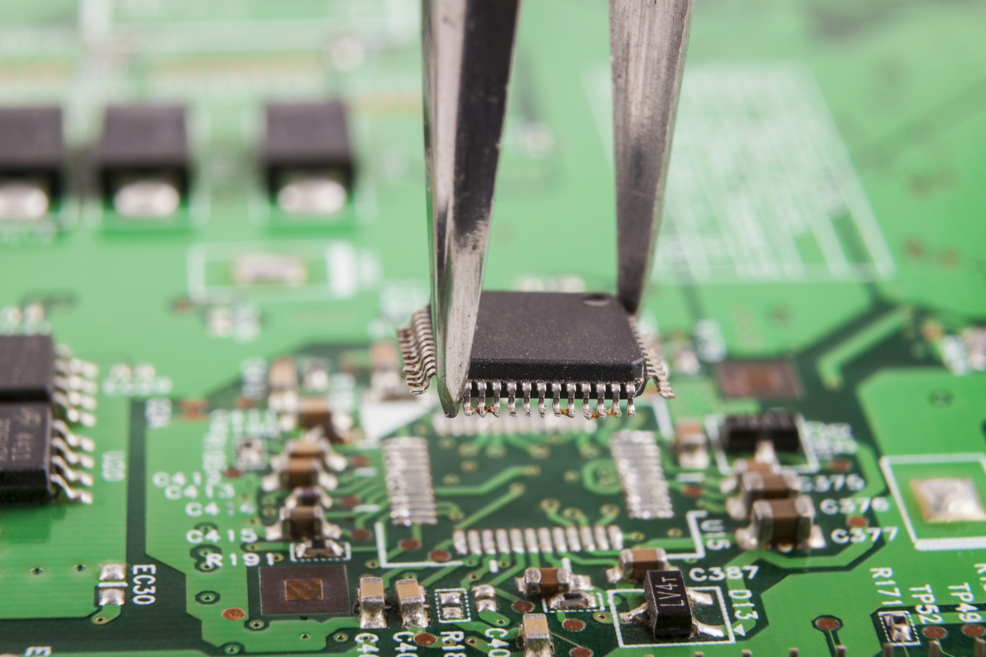
- The ubiquitous green color in solder mask is a fusion of tradition and practicality. Historically, green solder masks were used because the earliest solder mask resins had naturally green properties. As the electronics industry standardized, green solder mask became the default material, largely because of the precedent set by these early resins.
- On the practical side, the green solder mask provides excellent contrast with the white screen legend used to mark PCB components, making it easier to inspect and assemble the board. The human eye is particularly sensitive to green light, making it easier to spot defects or misalignments in complex circuit patterns. Additionally, under the bright lights of checkpoints, green surfaces tend to be less stressful on the eyes than other colors.
- In addition, green solder mask has excellent optical properties. It allows for clear inspection of traces and pads under a microscope without much glare. Additionally, many automated optical inspection systems are optimized for green PCBs, as this has been the industry standard for many years.
- While technological advancements allow for a wider range of colors to be used without sacrificing performance, the industry still favors green for its proven reliability and ease of use in the manufacturing process. Therefore, while not required, green remains a symbolic hue for the guardianship of circuits and a testament to the legacy of PCB design.
Solder Mask and Surface Mount Technology (SMT)
- In electronics assembly, solder mask acts as a strict watchdog, dictating where solder material can and cannot flow on a printed circuit board (PCB). This is especially important in SMT, where components are placed directly on the PCB surface and precise bonding is required to avoid solder bridging and ensure that tiny components are aligned with the fine structure of the board surface.
- The practical value of solder mask in SMT is also reflected in its role as a protective measure against poor solder paste registration. It helps define the solder paste deposition area for each mounting pad, which is necessary to prevent solder from connecting to adjacent circuit components, which can be catastrophic with the inherently microscopic scale of SMT.
What is the difference between solder mask and copper pad?
- In the intricate realm of printed circuit board (PCB) fabrication, the distinction between solder mask and copper pad is a study in contrast, both in function and form. The copper pad serves as the precise locus for electrical connectivity, a foundational platform upon which components are affixed. It is the elemental conductor, an archipelago of exposed metal on the PCB surface, to which the solder adheres during the assembly process.
- Conversely, the solder mask is the PCB's custodial layer, an insulative overcoat that enshrouds the substrate, safeguarding the myriad conductive traces that meander between the copper pads. This mask acts as a definitive boundary, precluding the solder from encroaching upon the interstitial spaces that must remain electrically isolated to avert inadvertent circuit paths.
- The copper pad is often revealed through apertures in the solder mask—a deliberate fenestration—allowing the metallic surface to interface with the solder and component leads. This deliberate exposure is critical for the establishment of secure and conductive joints in the assemblage of electronic components.
- In essence, the copper pad and solder mask are complementary components within the PCB architecture: the former is the designated site of electrical connection, while the latter is the protective overture that ensures the integrity and functionality of the entire electronic tableau.
Solder Mask and Environmental Compliance
Modern solder masks are designed to be compatible with lead-free soldering practices, an important step in reducing reliance on lead, a toxic element with well-documented environmental and health risks. This compatibility is critical as the electronics industry continues to transition to lead-free solder due to regulations such as the Restriction of Hazardous Substances Directive (RoHS). , minimizing the ecological footprint of PCB manufacturing. Advances in solder mask formulation have led to the development of materials that are free of volatile organic compounds (VOCs) and hazardous air pollutants (HAPs). These new compositions help reduce toxic emissions during the curing process and comply with industry and global environmental safety standards
Conclusion
The journey of the solder mask from a humble guardian of circuitry to a standard-bearer for environmental compliance is emblematic of the broader transformation within the electronics industry. It is a shift that acknowledges our dual responsibility: to innovate and to conserve. As we look towards the horizon, the solder mask stands not only as a protector of our technological endeavors but as a beacon guiding us towards a greener, more sustainable future.
