
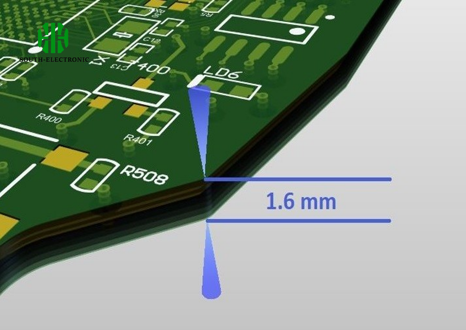
Ever wrestled with mysterious PCB assembly fails? That innocuous 1.6mm thickness isn’t random—it’s an engineering tightrope walk between rigidity and chaos. Ignoring it risks warped boards or connector nightmares. Let’s decode why this unassuming dimension rules the electronics jungle.
1.6mm emerged as the industry’s "Goldilocks thickness" because it balances mechanical stability, manufacturing economics, and compatibility with standard components/connectors—preventing SMT disasters while avoiding unnecessary bulk or cost for most applications.

But why did this magic number win the standards war? Stick around—we’re tearing down cost myths, warping horror stories, and revealing when to break from tradition.
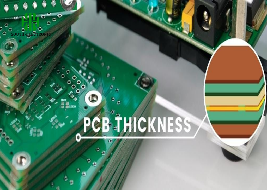
How to choose PCB thickness?
Choosing PCB thickness feels like navigating a minefield? A wrong pick risks cracked connectors or resonant failures. Panic sets in when boards flex mid-assembly. Relax—your thickness checklist starts with three non-negotiables.
Prioritize mechanical stress (enclosures/connectors), layer count (signal integrity needs), and thermal demands. Thicker boards (≥2.0mm) suit heavy components; thinner (≤1.0mm) optimize flex/wearables. Always simulate thermal expansion first.

Key Selection Strategy
Never decide in isolation. Cross-reference these factors:
-
Mechanical Load Analysis
Test fit in housings—PCIe cards demand 1.6mm slot compatibility, while consumer gadgets tolerate 0.8mm. -
Impedance & Signal Layers
High-speed designs? Thinner dielectrics control impedance but require stricter thickness tolerances. -
Thermal Stress Points
Copper distribution ratios below 70% risk warping during reflow. Validate via this decision matrix:
| Factor | When Thinner (1.6mm) | |
|---|---|---|
| Bending Stress | Wearables ✅ | Server boards w/ heatsinks ✅ |
| Cost Sensitivity | High-volume ✅ | Low-volume / RF ❌ |
| Via Reliability | Requires micro-vias ✅ | Handles standard aspect ratios ✅ |
Bottom line: Prototype early. A $200 simulation prevents $20k re-spins.
Can thinner PCBs save cost?
Hailed as cost-savers, ultra-thin PCBs tempt designers—till warping shreds yield rates. Thinner ≠ cheaper when reflow ovens buckle 0.4mm boards into potato chips. The real savings hide in overlooked details.
Thinner PCBs reduce material costs by ~15% but risk higher failure rates during assembly and testing. Net savings occur only for ultra-high-volume products (>10k units) with optimized processes—otherwise, thicker boards offset waste.

Cost vs. Risk Tradeoff
Dig deeper with these realities:
-
Material Savings Myth
Cutting core thickness 50% saves $5/㎡, but doubling scrapped panels loses $300/batch. Always calculate effective cost/unit. -
Tooling Incompatibility Taxes
0.6mm boards jam conveyorized test fixtures designed for 1.6mm—forcing $15k+ retrofit costs. -
Hidden Failure Costs
Thin laminates crack under BGAs during drop tests. Reliability fallout costs 200x initial savings.
Case in point: A drone client switched to 1.0mm boards expecting 12% savings—only to bleed 31% from warped SMT batches. Stick above 1.0mm unless you control every process variable.
That subtle board bend during reflow? It morphs into tombstoned resistors or invisible micro-cracks. SMT warping is PCB hell—and thickness is ground zero. Here are five nightmares I’ve autopsied.
The critical warping failures are: asymmetrical copper layers causing oven curl; <0.8mm boards buckling in fixtures; mixed-thickness panels; thick heatsink imbalances; and thermal expansion mismatches from inadequate Tg materials.
Dissecting Warp Disasters
Each failure mode reveals design blind spots:
-
"Potato Chip" Effect
Boards 12 layers induces curl. Symmetry is non-negotiable. -
Stackup Thermal Implosion
Mixing FR-4 (Tg 140°C) and polyimide in >2.0mm boards creates shear stress. Stick to one Tg rating. -
Heatsink Gravitational Warp
Big copper pads pull thin boards downward mid-cooling. Use 3.0mm tolerate 200W dissipation; 500Hz. Test deviations: under 2.0mm, failure rates double.
Rule: Specify extremes early. Changing thickness last-minute forces re-qualifying connectors, heat sinks, and EMI shields—costing weeks.
Conclusion
1.6mm hit PCB sweet-spot status by harmonizing rigidity, cost, and compatibility. But know when to break ranks—exotic thicknesses solve extreme challenges, rarely daily designs.

