
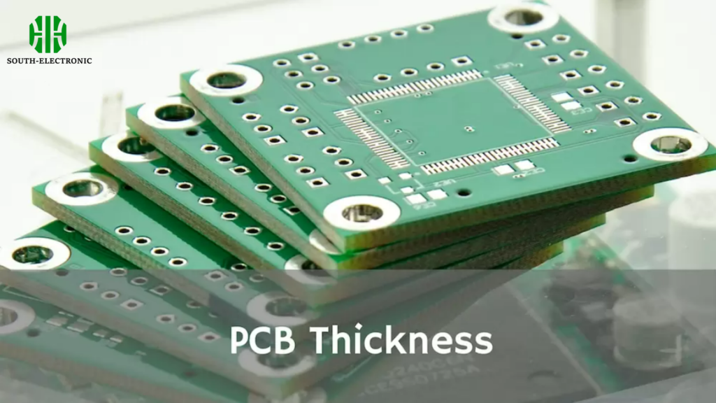
What is Standard PCB Thickness?
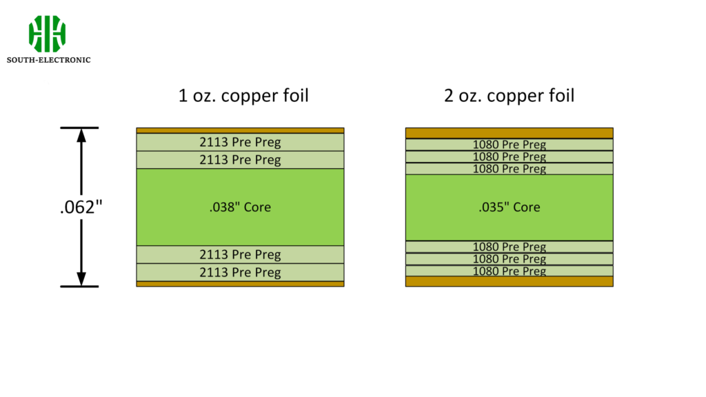
Most PCBs (Printed Circuit Boards) are about 1.6mm (0.063 inches) thick. That’s the standard thickness. It’s the most common thickness used all over the world. The standard that governs PCB thickness is IPC-2221A. It’s a standard for designing printed boards. It includes standards for board thickness. However, PCBs can be made thinner or thicker depending on the application’s specific requirements.
How Thickness is a 2-layer PCB?
PCB generally adheres to the standard thickness of 1.6 mm. However, depending on specific application requirements and constraints, A 2-layer PCB typically adheres to the same standard thickness of 1.6mm. This thickness includes the substrate and the copper layers on both sides.
Common PCB Thickness Standards and Applications:
| PCB Type | Standard Thickness | Application |
|---|---|---|
| Single-layer PCB | 1.6mm | General electronics |
| Double-layer PCB | 1.6mm | Consumer electronics, industrial |
| Multi-layer PCB | 0.8mm – 2.4mm | High-frequency circuits, complex devices |
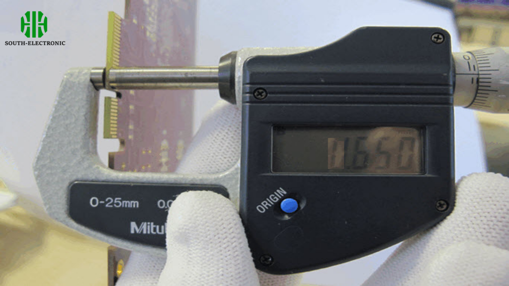
How is PCB Thickness Measured?
PCB thickness is measured using either a micrometer or a caliper. These tools will give you an accurate measurement of the total thickness of the board, including the substrate and the conductive layers. The measurement is usually done in millimeters or inches, and you should take measurements at multiple points across the PCB to make sure the thickness is consistent.
Factors Influencing PCB Thickness
Several factors can influence the decision on PCB thickness, including:
- Application Requirements: High-power or high-temperature applications may require thicker PCBs for better heat dissipation and mechanical strength.
- Space Constraints: In compact electronic devices like smartphones or tablets, a thinner PCB might be necessary to fit into the limited space.
- Layer Count: More layers in a PCB generally necessitate increased thickness to accommodate the additional layers of copper and insulation.
- Cost Considerations: Thicker PCBs typically use more material, which can increase the overall cost of production.
- Electrical Requirements: The voltage and current levels, as well as impedance requirements, can dictate the need for adjustments in PCB thickness to ensure safe and reliable operation.
These answers provide a comprehensive look at PCB thickness standards, ensuring clarity and depth to meet the needs of individuals engaged in electronics design and manufacturing.

