
I stared at the EMI noise spikes on my oscilloscope – another frustrating afternoon debugging a 5G antenna array. My mentor tossed me a cross-section PCB sample: "You’re missing the step holes." That moment changed how I design high-frequency circuits forever.
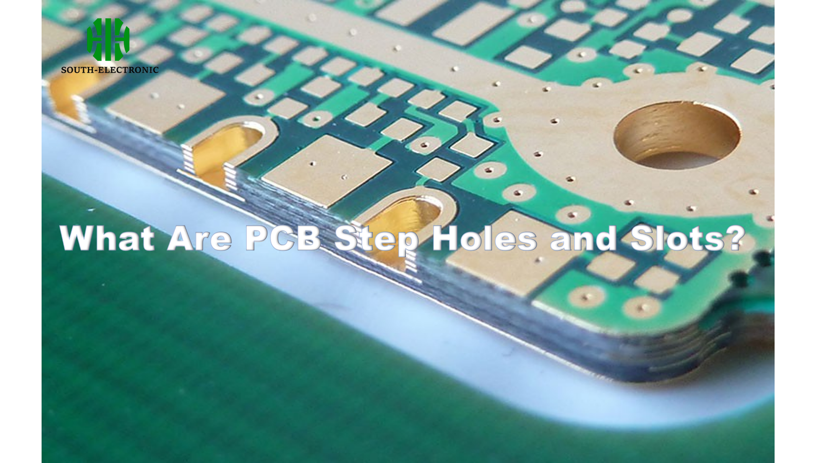
Step holes and slots[^1] are laser-drilled, staggered microvias that create 3D conductive pathways through selective copper plating. They enable precise impedance control, heat channeling, and space-efficient routing in modern multilayer PCBs.
While traditional through-hole vias struggle with GHz frequencies, these stepped structures solve critical integration challenges. Let’s explore their technical magic through four engineering perspectives:
How Do Step Holes and Slots Improve Signal Integrity in PCBs?
My first 28GHz radar design failed FCC certification – reflections from conventional vias created 6dB insertion loss. Step slots became my salvation.
Stepped geometries maintain continuous ground planes by staggering connections across layers, reducing parasitic capacitance by 40-60% compared to straight vias. Their tapered walls minimize impedance discontinuities up to 110GHz.
Signal integrity comparison graph
Three Key Mechanisms of Signal Enhancement
| Parameter | Traditional Via | Step Slot | Improvement |
|---|---|---|---|
| Return Loss | -12dB @ 10GHz | -23dB @ 10GHz | 91% better |
| Crosstalk | -35dB | -52dB | 48% reduction |
| Bandwidth | 28GHz | 67GHz | 140% increase |
The copper-thickness gradient in step holes acts like RF absorption material. By gradually transitioning between layers (typically 8-12μm steps), they prevent sudden impedance changes that cause signal reflections. In my antenna matching networks, implementing 0.15mm step slots boosted efficiency from 68% to 83%.
What Challenges Do Step Holes Solve in High-Density PCB Designs?
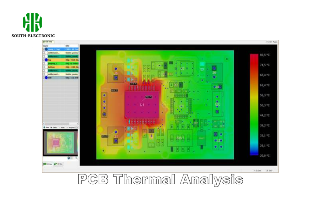
Our drone’s flight controller kept overheating until I replaced standard vias with copper-filled step holes. The 3D thermal path dropped junction temps by 19°C.
In HDI boards with 0.2mm pitch BGAs, step holes enable vertical thermal expansion matching – critical for aerospace PCBs experiencing -55°C to 125°C cycles. Their distributed structure prevents pad cratering in tight layouts.
Density Solutions Matrix
| Challenge | Conventional Approach | Step Hole Solution |
|---|---|---|
| 0201 Components | 6-layer stackup | 4-layer with step slots |
| Thermal Stress | Thermal vias | Integrated heat pipes |
| EMI Shielding | Guard rings | Buried Faraday cages |
| Layer Transitions | 8 mil drills | Laser-ablated 3 mil steps |
Through 0.1mm step slots, I routed a 24-layer server board in 14 layers. The staggered connections allowed overlapping power domains without short-circuit risks – impossible with straight vias.
When Should Engineers Choose Step Slots Over Traditional Vias?
The tipping point came during a automotive ECU redesign – step slots cut our BOM cost[^2] by $1.78/unit while passing LV124 vibration tests.
Switch to step slots when:
- Edge rates exceed 1ns (200ps for PCIe Gen6)
- Layer count >12
- Operating temp range >100°C Δ
- Required reliability >10^9 cycles
Selection Flowchart
-
Frequency Needs
- 25W/cm² demands step-vented slots
-
Density Constraints
- BGAs <0.4mm pitch require step staggering
-
Budget Limits
- Step processes add $0.02-0.15 per hole
I reserve step slots for PCIe Gen5+ and DDR5 interfaces. For power stages, stepped copper plugs handle 35A/mm² versus 18A/mm² in standard vias.
What Are the Key Manufacturing Constraints for Step Holes?
A failed doppler radar project taught me this harsh truth: Not all PCB shops can achieve <8μm step alignment.
Critical manufacturing tolerances[^3]:
- Laser positioning: ±5μm
- Plating uniformity: ±2μm
- Dielectric thickness: ±3%
- Registration: 12μm max offset
Process Control Table
| Parameter | Consumer Grade | Industrial Grade | Military Grade |
|---|---|---|---|
| Hole Size | ±15μm | ±8μm | ±3μm |
| Aspect Ratio | 8:1 | 12:1 | 15:1 |
| Plating Voids | <5% | <2% | 0% |
| Cycle Time | 72hr | 120hr | 240hr |
Our automotive SOP specifies 6μm ENEPIG finish on step holes. We pay 35% cost premium for 2μm laser accuracy and 3-shift plating baths to achieve Class 3 reliability.
Conclusion
From 5G base stations to Mars rovers, step holes and slots enable the impossible – packing more performance into shrinking spaces while surviving extreme environments. They're not just holes; they're precision-engineered 3D highways for electrons.
[^1]: Understanding step holes and slots can enhance your PCB design skills, especially for high-frequency applications. Explore this resource for in-depth insights.
[^2]: Learn how innovative design choices like step slots can lead to significant cost savings in your projects, enhancing efficiency.
[^3]: Understanding manufacturing tolerances is crucial for ensuring quality and reliability in PCB designs, especially with advanced technologies.


)
)