
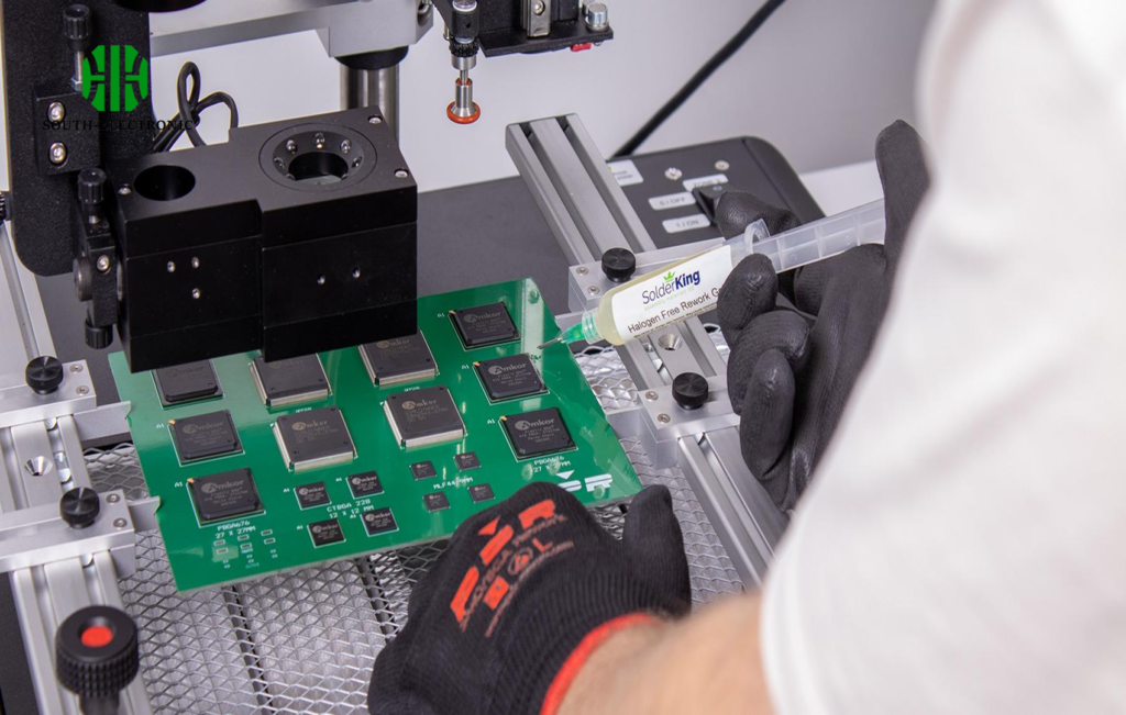
Like many engineers during R&D validation, I like to send boards out to assembly houses for SMT prototype runs to save time. But let me tell you, I’ve had my share of frustration. Board arrives, I power it up… and nothing. Shorts. Opens. Basic functionality testing fails. Now comes the headache: Was this my design mistake? Or did the assembly shop mess it up? Finger-pointing costs time and money every time.
After burning cash on one too many bad batches, I collected information on the most common SMT assembly problems from the trenches. Understanding these has saved me countless "back to the drawing board" moments. Here’s what you need to watch for:
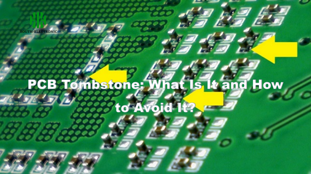
1️⃣ Defect 1: "Tombstoning"
What’s Happening: A small resistor or capacitor (like a 0603 or 0402) lifts completely off one pad and stands straight up during reflow soldering. Think of a miniature gravestone.
Why It Happens & How to Fix It:
This happens mainly when one end of the part melts and "wets" quicker and stronger than the other end. Think of it as an unbalanced tug-of-war pulling the part upward.
Tombstoning is especially tricky for very tiny parts (like 0201 or 01005 sizes). The forces are smaller, and imbalances make everything worse. It really shows how vital thermal balance is. A pad sitting over a huge copper plane is like attaching it to a giant ice cube. That pad stays cooler longer. The partner pad heats up fast, melts quickly, and develops strong surface tension. This imbalance can easily flip the little part on its end before the cooler pad even gets warm. Fixing this often means breaking that copper pour connection with thermal spokes – making the "cool" pad less connected to the giant heat sink. Sometimes a small cut in the ground plane near the pad also helps. Getting the paste print right is harder on tiny features.
The stencil must be laser-cut well and stick tight to the board surface during printing. Any gap means poor paste transfer. Using nitrogen gas inside the reflow oven can sometimes improve wetting, which might help prevent this issue.
2️⃣ Defect 2: Solder Beads / Solder Balls
What’s Happening: Tiny balls of solidified solder sticking to the board surface, not where they belong. They sometimes cluster near components, especially under fine-pitch chips, or sit off to the side looking like trapped metal droplets. Worst case? They cause hidden shorts you discover only when the board fails.

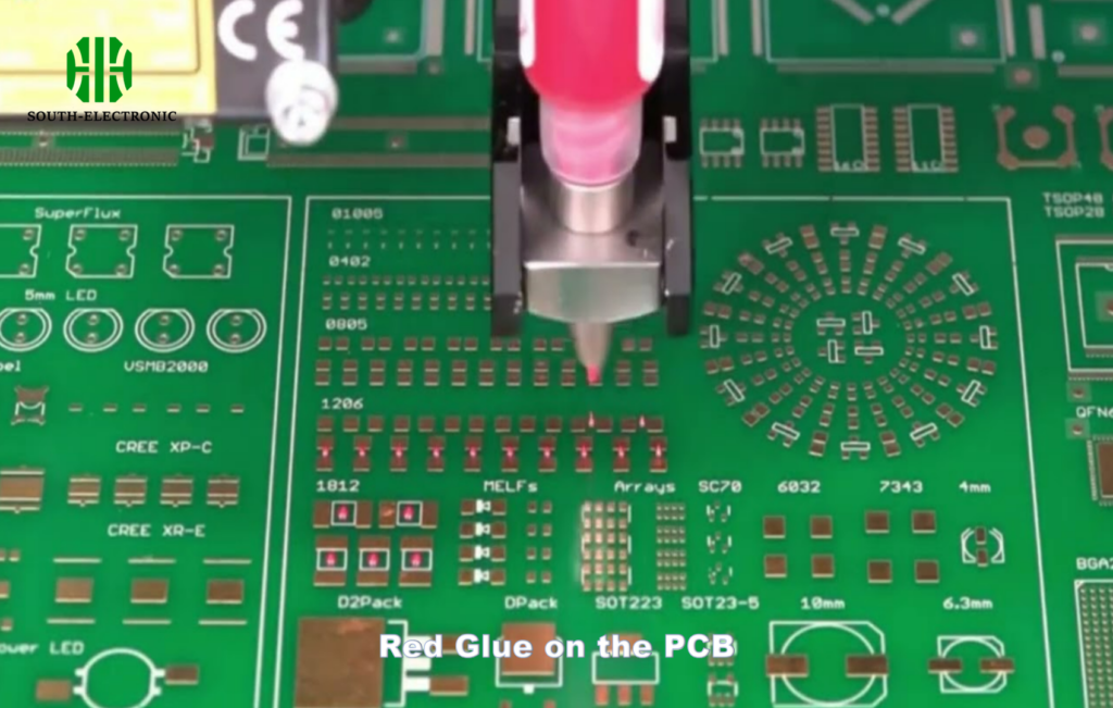
Solder balls look simple, but they often reveal deep process control problems. Moisture in the paste is a killer. Paste straight from the fridge, used without letting it sit on the bench for the required 4-8 hours (check specific paste specs!), will have absorbed water from condensation. When paste hits high heat, that water boils instantly. Trapped flux gas expands the melt violently – launching tiny droplets of still-molten solder far from the pad. These solidify instantly as balls. High metal content paste usually does better.
Cleaning is critical too – residues under components or on pads can create spots where wetting fails, pushing molten solder to pile up elsewhere as balls. Nitrogen inerting the reflow furnace helps reduce oxidation, meaning less flux is burned trying to clean surfaces. This allows lower activity fluxes to work and reduces spattering. For dense boards or BGAs, getting clean prints under components takes a very flat stencil and a good printing machine. I sometimes ask about adding "solder ball guards" to the stencil design – small dams next to pads to stop escaping paste.
3️⃣ Defect 3: Solder Bridging
What’s Happening: Solder forms an unwanted short circuit between adjacent component pins or pads. This creates obvious electrical shorts. Bridges are common on tightly-spaced IC pins (like QFPs) and under tightly-packed BGAs.
Dive Deeper: Bridging on ultra-fine pitch components (think < 0.4mm pin spacing) is an ongoing battle. Every micron matters. The stencil design becomes incredibly important. Often, "reduced aperture" stencils are used – printing narrower and slightly shorter pads deliberately. This leaves a small gap between the paste and the solder mask wall separating pads. "Nanocoated" stencils with an ultra-smooth surface and sometimes anti-stick coatings help get a clean paste release. Paste type is key here too – "Type 4" or "Type 5" solder pastes have much finer metal powder particles designed to give sharp prints for these tight areas.
Printer calibration is constant work – boards must clamp flat, squeegee pressure uniform, print speed controlled. For BGAs, bridges are catastrophic. X-ray inspection helps spot them. Often, solder paste volume on the board pad for the tiny BGA balls is critical – too much paste leads to collapse and bridging during melt. Getting clean stencil separation without dragging paste requires careful snap-off distance adjustment. Poor pad finish on the PCB, like inconsistent HASL (HOT AIR SOLDER LEVELING), can cause solder to flow unevenly and cause bridges. ENIG finish is generally preferred for fine pitch and BGAs.
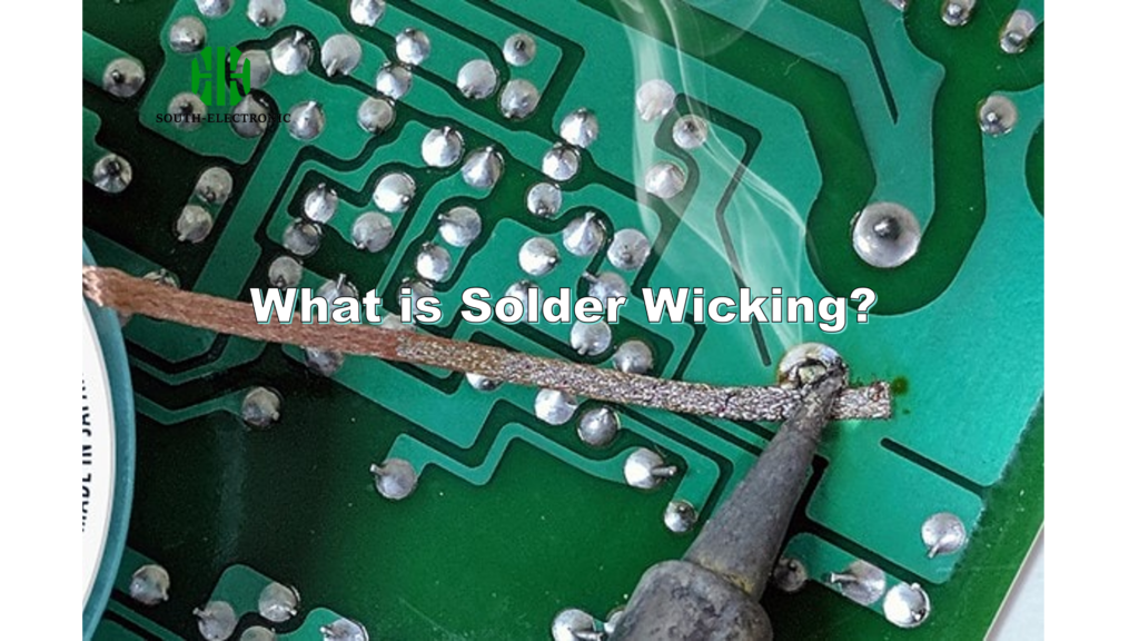
4️⃣ Defect 4: "Wicking"
What's Happening: Instead of forming a nice joint on the pad, the molten solder completely crawls up the component lead. This leaves the actual pad dry and poorly soldered. You'll mostly see this with through-hole parts during reflow, but surface mount pins can do it too.
Wicking feels like gravity stopped working for solder. It's all about surface tension driven by heat differences. Thick copper pins act like heat highways, racing ahead of the PCB material. Cold pads mean weak solder wetting down below. The solder alloy wants to stick to the hottest metal surface it touches first. In extreme cases, solder will completely desert the pad and fully coat the pin up to the component body. This creates terrible mechanical connections. Preventing wicking means controlling the heating environment carefully. Vapor phase reflow is notorious for this because the heat transfer method can exaggerate differences. Using IR reflow or forced convection reflow ovens gives more control.
Preheating stages are critical – getting everything in the 100-150°C range consistently before the big heat push. Sometimes, using a slightly lower peak temperature or slower ramp helps balance things. For designs with big, power-hungry connectors or pins, consider adding small thermal breaks near the pad connection point to slow down the heat race. If you see wicking consistently on certain pins, check their copper connection – they might be isolated copper columns acting like perfect heat antennas drawing solder away from the pad.
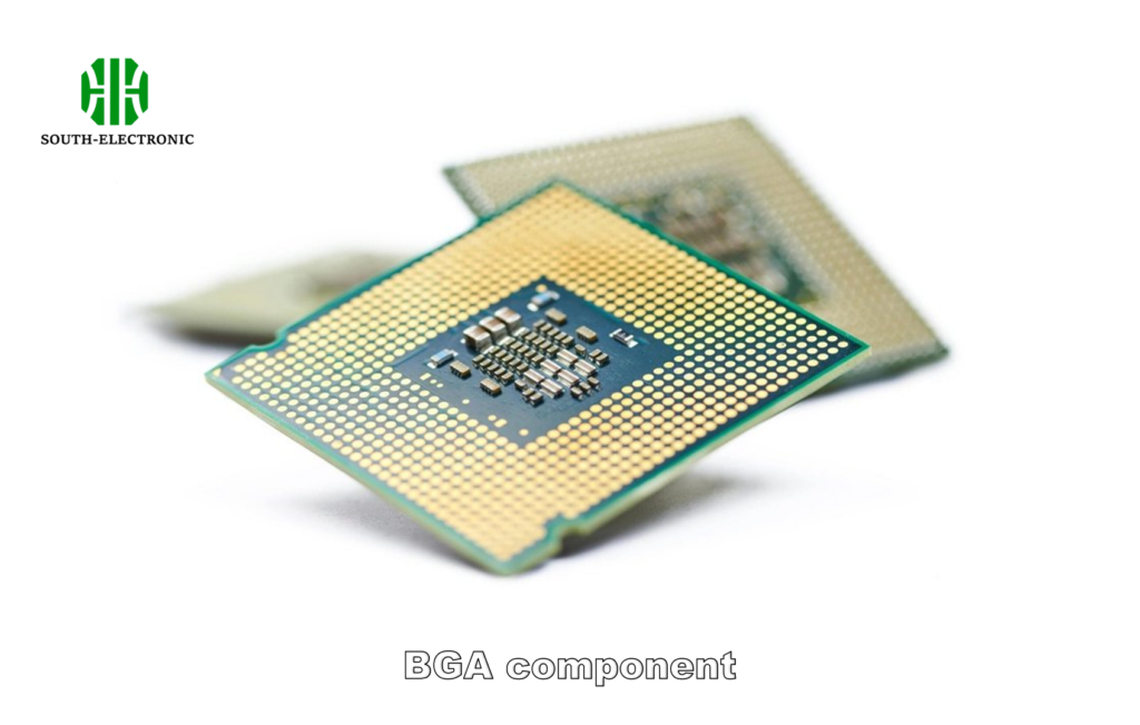
5️⃣ Defect 5: BGA Nightmares
What's Happening: BGA (Ball Grid Array) joints hide under the chip. X-rays can reveal problems like:
- Bridging: Neighboring balls melt together (very hard to spot without X-ray!).
- Head-in-Pillow (HiP): The BGA ball doesn't fully melt into the pad solder. It touches but doesn't properly fuse – like a head resting on a pillow without sinking in.
- Cold Solder: Joints look grainy and dull because they never fully melted.
- Voids/Bubbles: Empty pockets trapped inside the solder joint.
- Cracked Joints: Fractures from stress after cooling.
- Contamination: Dirt or oxidation blocking the connection.
BGAs are tough because you can't visually inspect them. Head-in-Pillow has become way more common with lead-free solder needing higher temperatures. Those temperatures often cause PCB warpage, literally bending the board away from the BGA during the most critical melt phase. Imagine trying to kiss someone who suddenly leans back – you barely touch! Even tiny amounts of warping cause HiP. Nitrogen in the reflow oven sharply reduces oxidation on balls and pads. Oxidation creates a barrier solder won't wet properly. Vacuum reflow systems are popping up to reduce voids (bubbles) – they pull trapped gases out during melting. For voids, focus on pad design and paste volume. Paste printed over vias will bubble violently as air escapes during reflow. Stencil designers must avoid placing paste apertures directly over via holes.
For reliability, controlling the cooling rate helps. Cooling too fast makes joints brittle and prone to cracking when the board twists in later use. Cleaning boards before placement gets overlooked – tiny fibers or dirt prevent good ball-to-pad contact. BGA assembly requires meticulous cleanliness. X-ray inspection is critical. But not all X-ray machines show HiP well. Angle shots are needed to spot that faint separation line between ball and pad solder. Getting BGAs right pushes every part of the assembly process to its best.
💡 The Real Fix: Know Your Shop
Finding these defects isn't just technical detective work – it's about avoiding blame games and delays. I don't want weeks wasted arguing with an assembly house about who is at fault for bad solder paste. So here's how I approach it:
-
I Draw First: Before sending files out, I audit my design like it committed a crime. I use DFM (Design for Manufacturability) tools. Things I check:
- Pad symmetry and thermal balancing for small passives
- Solder mask dams between tight IC pins (to block bridges)
- Thermal reliefs on pads connected to ground planes
- Pad size vs. component specifications
- Via placement under BGA pads (usually forbidden!)
- Clear assembly notes on inspection requirements
-
I Talk Second: I don't just email my files and wait. I call the shop's process engineer:
- What solder paste brand/type do they use? Is it fresh?
- Do they profile the oven for each board type? How?
- What stencil design rules do they follow? (Thickness, aperture reductions)
- Will X-ray inspect BGAs? And at what resolution?
- Ask for their standard reflow profile – does it match my paste specs?
-
I Prepare to Test: I design test points everywhere. For every power rail. For critical signals near BGAs. For network connections. Boards come back – first thing I do? Basic continuity test on every net before powering up. Finding a short between power and ground takes seconds with a multimeter. Finding it after populating the board? That might cost hundreds in fried parts.
Conclusion
SMT isn't magic. It's physics controlled by good design and precise process. Focus on heat balance, paste quality, cleanliness, and controlled heating – most defects vanish. Spending hours fixing my design before fabrication saved me weeks of heartache later. Finding a shop willing to share their process details? That’s pure gold. The reality is simple: Good SMT needs design and assembly to work together as one team.

