
Telecom & Networking PCBA Services
Optimized for cost, quality, and fast iteration
We provide reliable PCBA solutions for telecom and networking applications, supporting startups and OEMs with stable quality, flexible MOQ, and consistent performance from pilot run to volume production.
Telecom & Networking PCBA Capabilities
Telecom & Networking PCBA Capability
-
ASSEMBLY TYPE
SMT / DIP / Mixed Assembly
-
PRODUCT TYPES
Telecom equipment · Networking devices · Routers · Switches · Signal processors
-
COMPONENT SOURCING
Turnkey / Partial Turnkey · Global sourcing · Obsolete & hard-to-find components
-
SUPPORTED PACKAGES
BGA · QFN · QFP · LGA · 0201 / 01005 components
-
BOARD TYPES
Rigid PCB · Rigid-Flex PCB · HDI PCB
-
BOARD SIZE
≤ 610 × 1200 mm (24 × 48 inch)
-
BOARD THICKNESS
0.2 mm – 8.0 mm
-
TESTING & INSPECTION
AOI · X-ray · ICT · Functional Test · Aging Test (on request)
-
PRODUCTION VOLUME
Prototype · Small batch · Mass production
Why Choose Us for Telecom & Networking PCBA
We support telecom and networking companies with reliable PCBA solutions,
from early prototypes to stable mass production.
Every telecom PCBA project is meticulously reviewed by our engineers to assess BOM, DFM, and test requirements before production.
Consistent assembly quality across batches, ensuring reliability for pilot runs and long-term volume production.
Expertise in managing intricate layouts, fine-pitch components, and complex telecom device assemblies.
Clear technical communication and fast response for overseas engineering and procurement teams.
Quality Control & Certifications for Telecom & Networking PCBA
PCBA for Telecom Router
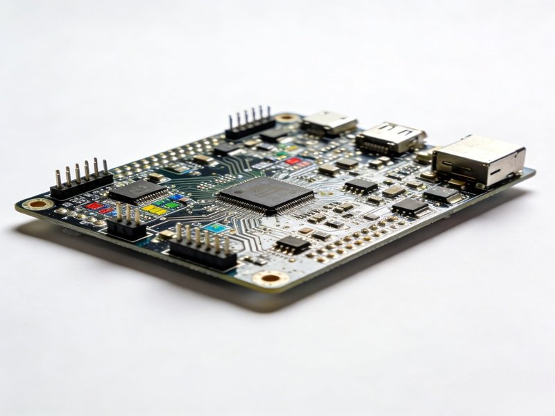
Application
Key Specs
Challenge
Result
PCBA for Networking Switch
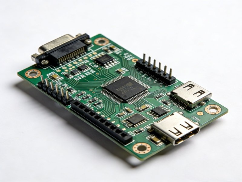
Application
Key Specs
Challenge
Result
PCBA for Telecom Signal Processor
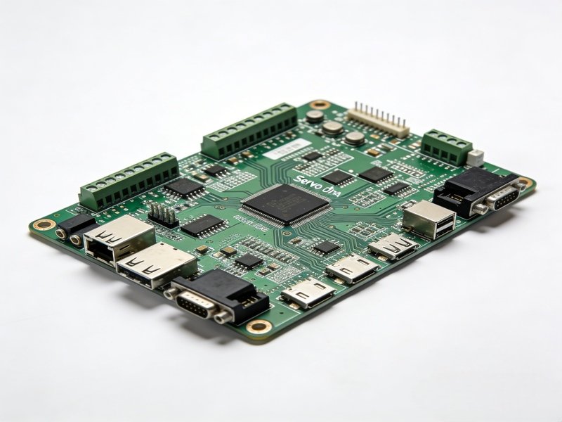
Application
Key Specs
Challenge
Result
Common Questions
Most Popular Questions
Can you handle complex layouts and fine-pitch components?
Yes, extensive experience in managing complex layouts and fine-pitch components, ensuring precise assembly and high-performance results.
What certifications do you hold that ensure quality and compliance?
We operate under ISO 9001, ISO 13485, and IATF 16949 standards for rigorous quality and compliance.
What is the lead time for prototype PCBA orders?
Lead time for prototype orders is typically around 2 weeks, depending on component availability and specific project requirements.
Do you offer component sourcing services?
Yes, we provide comprehensive component sourcing, including turnkey and partial turnkey options.
What files are required to get an IoT PCBA quotation?
Send Us a Message
The more detailed you fill out, the faster we can move to the next step.
