
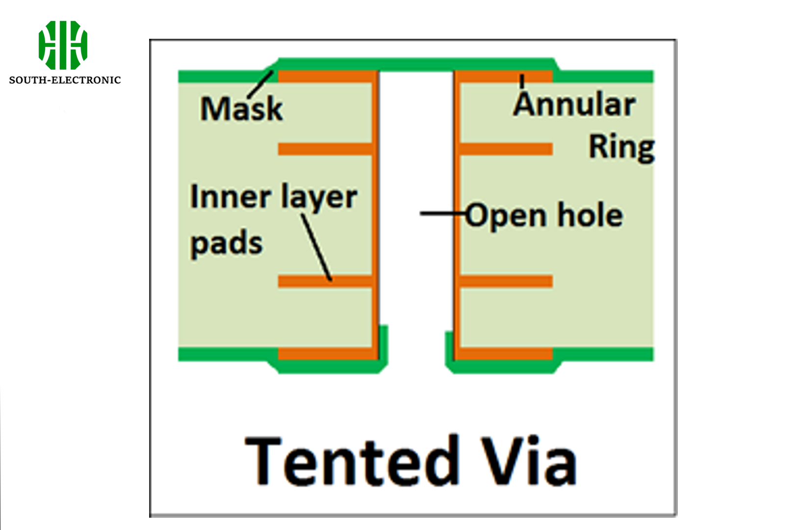
What is Tenting of Via in PCB?
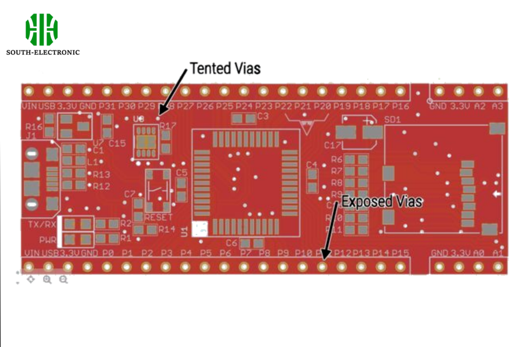
Tent vias are vias covered with a solder mask to enclose or skin over the opening. Tenting of via in PCB refers to the process of covering a via with a solder mask or similar nonconductive material. A via is a plated hole that allows signals to pass between different layers of a PCB. By tenting a via, both the pad and hole are covered, which helps in protecting the via from contaminants and enhancing the overall durability of the PCB.
Benefits of Tented Vias
- Enhanced Insulation: Tenting vias provide better insulation between layers, especially when routing high-density traces.
- Avoiding Solder-Wicking Issues: It prevents solder from wicking into the via, which can cause solder bridging.
- Allowing Crossover Routing: Designers can route traces over the vias without worrying about exposure or shorting.
Via Tenting and Plugging
Via tenting and plugging are two different techniques used in PCB fabrication. While tenting involves covering the via with a solder mask, plugging involves filling the via with conductive or non-conductive material.
Differences Between Tenting and Plugging
| Aspect | Tenting | Plugging |
|---|---|---|
| Process | Covering via with solder mask | Filling via with conductive material |
| Purpose | Protect via from contaminants | Improve mechanical stability |
| Applications | General PCB protection | High-reliability applications |
Altium Via Tenting Rule
Altium Designer, a popular PCB design software, provides specific rules and guidelines for implementing tented vias. Designers can specify the level of tenting and ensure compliance with manufacturing standards.
- Open the PCB Rules and Constraints Editor.
- Navigate to the “Mask” category.
- Adjust the settings under “Tenting Vias” to either “Tent All Vias” or specify particular conditions based on your design needs.
- This configuration can help prevent potential issues like short-circuits and improve the overall durability and functionality of the PCB.
Tenting vias involves applying solder mask over the via to prevent solder, flux, or contaminants from accumulating in the via during assembly, which enhances PCB reliability and performance, particularly in high-density designs.

