
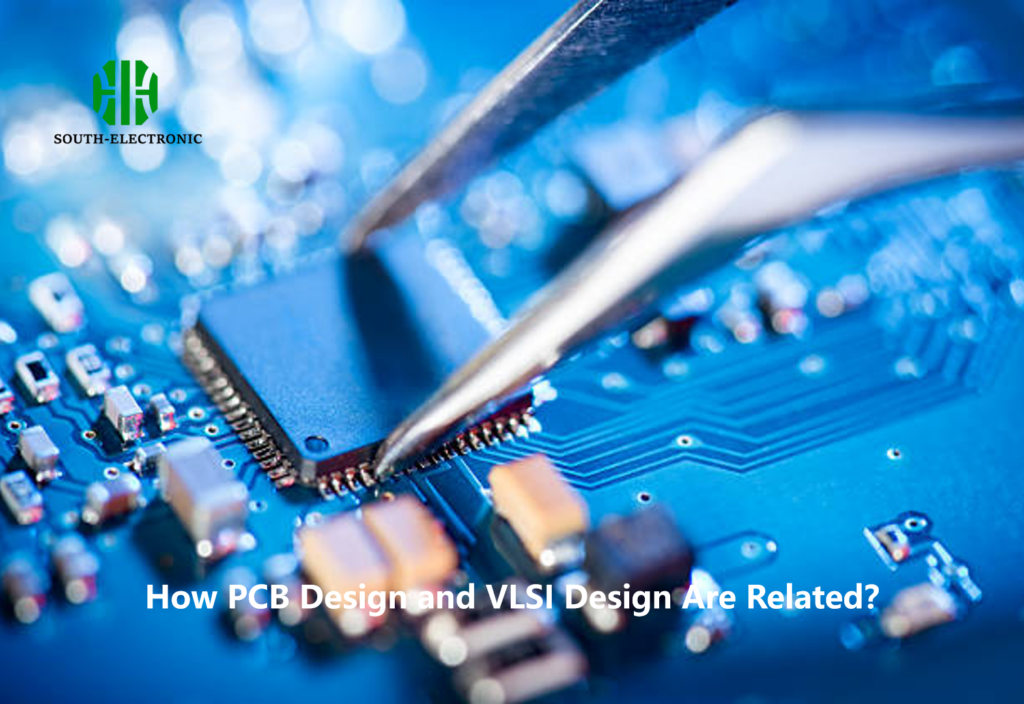
PCB design and VLSI design are two fundamental aspects of electronic device development. PCB design is about creating physical pathways for electrical components, while VLSI design is about packing millions of transistors onto a chip. Though they serve different purposes, they are interrelated in creating functional electronics.
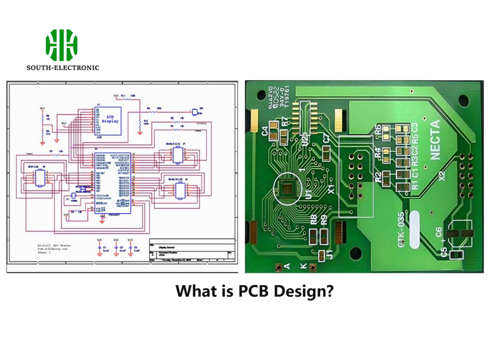
What is PCB Design?
PCB design is the process of designing the physical layout of a circuit board, which holds and connects all the components of an electronic device. PCB designers work on:
- Schematic capture: Creating a blueprint of the circuit’s electrical connections.
- Component placement: Ensuring efficient and reliable placement of electronic parts.
- Routing: Connecting components using copper traces.
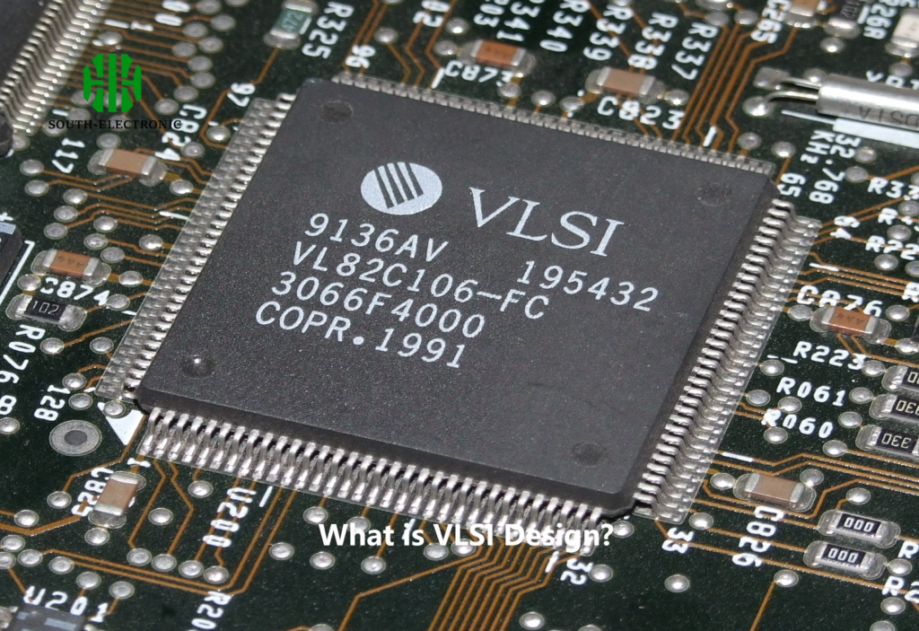
What is VLSI Design?
VLSI (Very Large Scale Integration) design is the process of integrating thousands to billions of transistors onto a single chip. This process changed the electronics industry by making integrated circuits (ICs) smaller and cheaper, while also making them faster. The VLSI process includes:
- Logical design: Creating a circuit that meets the functional requirements.
- Physical design: Mapping the logical components onto physical silicon.
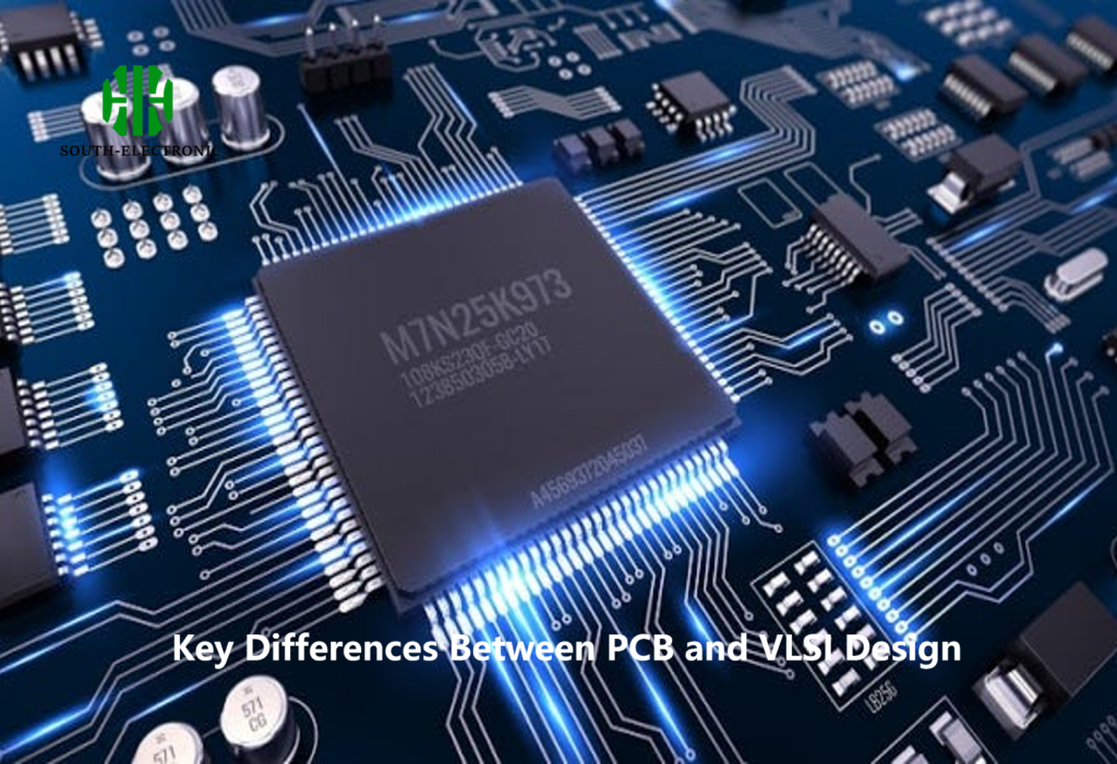
Key Differences Between PCB and VLSI Design
While PCB and VLSI design are closely related in the electronics world, they operate on different levels of abstraction.
| Aspect | PCB Design | VLSI Design |
|---|---|---|
| Scale | Board-level design with discrete components | Chip-level design with millions of transistors |
| Physical Layer | Focus on copper traces and components | Focus on silicon layers and logic gates |
| Process | Routing components on a PCB | Integrating components into a single silicon chip |
| Software Used | Altium, Eagle, KiCAD | Cadence, Synopsys, Mentor Graphics |
How PCB Design and VLSI Design Are Related?
PCB design and VLSI design are two important aspects of creating complex electronic devices like smartphones, computers, and embedded systems. VLSI design is all about creating efficient, compact chips, while PCB design is about connecting these chips to other components to form complete systems.
1. Interconnection of VLSI Chips in PCBs
VLSI chips are made to be used on PCBs. For example, processors, memory chips, and other ICs designed using VLSI are put on PCBs to make electronic systems that work.
2. Signal Integrity Between PCB and VLSI
When you’re designing PCBs that use VLSI chips, you’ve got to make sure that you maintain signal integrity. As the frequencies of the signals get higher and higher, you’ve got to be really careful about how you design your traces so you don’t get interference and signal degradation.
3. Power Distribution
When you’re designing a PCB or a VLSI chip, you’ve got to make sure that you distribute power properly. In VLSI, you distribute power at the chip level, and in PCB design, you distribute power at the board level. You’ve got to make sure that both of these things work together so that power gets to all the parts of the device that need it.
Comparison of PCB and VLSI Design Processes
| Design Process | PCB Design | VLSI Design |
|---|---|---|
| Design Goal | Connecting components on a board | Integrating multiple functions into a single chip |
| Primary Tools | Schematic capture tools | RTL design, synthesis, and layout tools |
| Design Challenges | Signal routing, thermal management | Power, speed, and area optimization |
| Manufacturing | Manufacturing of multilayer boards | Fabrication of silicon wafers and IC packaging |
Use Cases of PCB and VLSI Design
1. Consumer Electronics
Both PCB and VLSI design are important in consumer electronics like smartphones, laptops, and wearables. VLSI is responsible for creating the processors and memory units, while PCB design connects them with other components like sensors, antennas, and power supplies.
2. Medical Devices
In medical devices, VLSI chips often do important things, like keeping track of your vital signs in wearable health trackers. PCBs connect all the different parts of these devices, making sure they’re small, efficient, and work right.
3. Automotive Industry
ADAS, infotainment systems, and ECUs all rely on both PCB and VLSI design. VLSI design creates the chips for data processing, while PCB design ensures proper component integration.
Industry Trends in PCB and VLSI Design
1. 3D ICs and Multi-Layer PCBs
The move toward 3D ICs, where chips are stacked vertically, necessitates PCBs with multiple layers. This allows for greater interconnectivity and reduced signal delay, making devices faster and more efficient.
2. Automation in Design Tools
Both PCB and VLSI design tools are becoming more automated, with artificial intelligence (AI) and machine learning (ML) algorithms assisting in design optimization. This helps reduce human error and speeds up the time-to-market.
PCB design and VLSI design are two parts of the electronics industry. PCB design focuses on the physical interconnection of components, while VLSI design integrates a lot of logic into a single chip. Together, they form the backbone of modern electronics, from consumer gadgets to complex industrial systems.

