
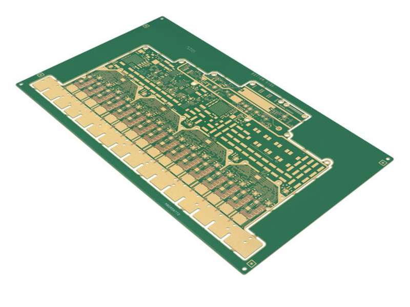
Custom Thick Copper PCB Manufacturing Services
Min trace 3/3 mil | ENIG / HASL | FR-4 & Aluminum | AOI & E-Test
We manufacture high-precision thick copper PCBs designed for demanding applications in power electronics, lighting, and industrial equipment, ensuring stable quality and consistent performance for repeat production.
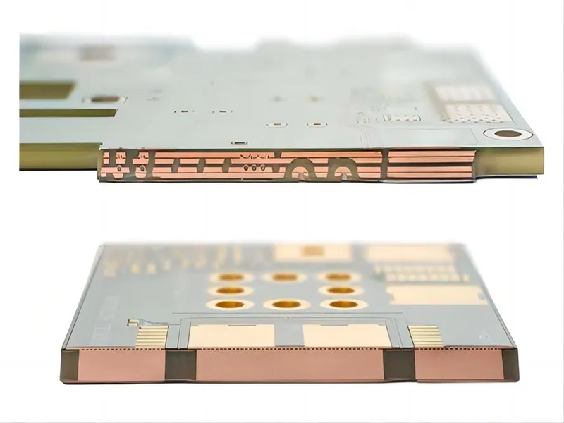
Thick Copper PCB Capabilities
Thick Copper PCB Process Capability
-
Layer Count
8 layers
-
PCB Dimensions
≤24*48inch(610*1220mm)
-
Materials Types
FR-4 | High Tg | Halogen-free | PTFE | Ceramic PCB | Metal substrate material
-
Material Brand
Lianmao|Shengyi| Taiyao| Nanya, Panasonic|Isola|Nelco|Rogers|Taconic|Arlon...
-
Board Thickness
0.2mm-8.0mm
-
Finish Treatment
Immersion Gold|Lead-free HASL|OSP|Immersion Tin|Immersion Silver|Thick Gold Plating|Silver Plating|Immersion Gold+OSP
-
Copper thickness
0.33 OZ-8 OZ
-
SolderMask Color
Green| Blue| Black|Yellow| Red|Purple| White...
-
Finish Treatment
Immersion Gold|Lead-free HASL|OSP|Immersion Tin|Immersion Silver|Thick Gold Plating|Silver Plating|Immersion Gold+OSP
Why Choose Us for Thick Copper PCB Manufacturing
We support engineers with reliable thick copper PCB manufacturing,
from prototype builds to stable repeat production.
Every thick copper PCB is meticulously reviewed by our engineers to ensure optimal thermal management, impedance control, and manufacturability before production.
We prioritize consistent quality across batches, delivering reliable performance for both prototypes and long-term production runs.
Skilled in handling high copper thicknesses, thermal dissipation, and precision manufacturing for demanding applications.
We ensure transparent technical communication and fast response times to effectively support overseas engineering and purchasing teams.
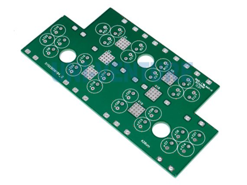
Related Project We Had Done
Thick Copper PCB for Industrial Lighting System
Application
Key Specs
Challenge
Result
Thick Copper PCB for Power Supply Unit
Application
Key Specs
Challenge
Result
Thick Copper PCB for Electric Vehicle Charging
Application
Key Specs
Challenge
Result
Quality Control & Certifications for Thick Copper PCB Production
Common Questions
Most Popular Questions
Can you provide prototypes for Thick Copper PCBs?
How do you ensure quality in your Thick Copper PCBs?
Are there specific materials you recommend for Thick Copper PCBs?
Do you offer design support for Thick Copper PCBs?
What is the minimum order quantity for Thick Copper PCBs?
Send Us a Message
The more detailed you fill out, the faster we can move to the next step.
