
As devices shrink to microscopic scales, a critical engineering dilemma emerges: How do we maintain electrical performance in vanishingly small spaces? The answer lies in a disruptive manufacturing miracle thinner than human hair.
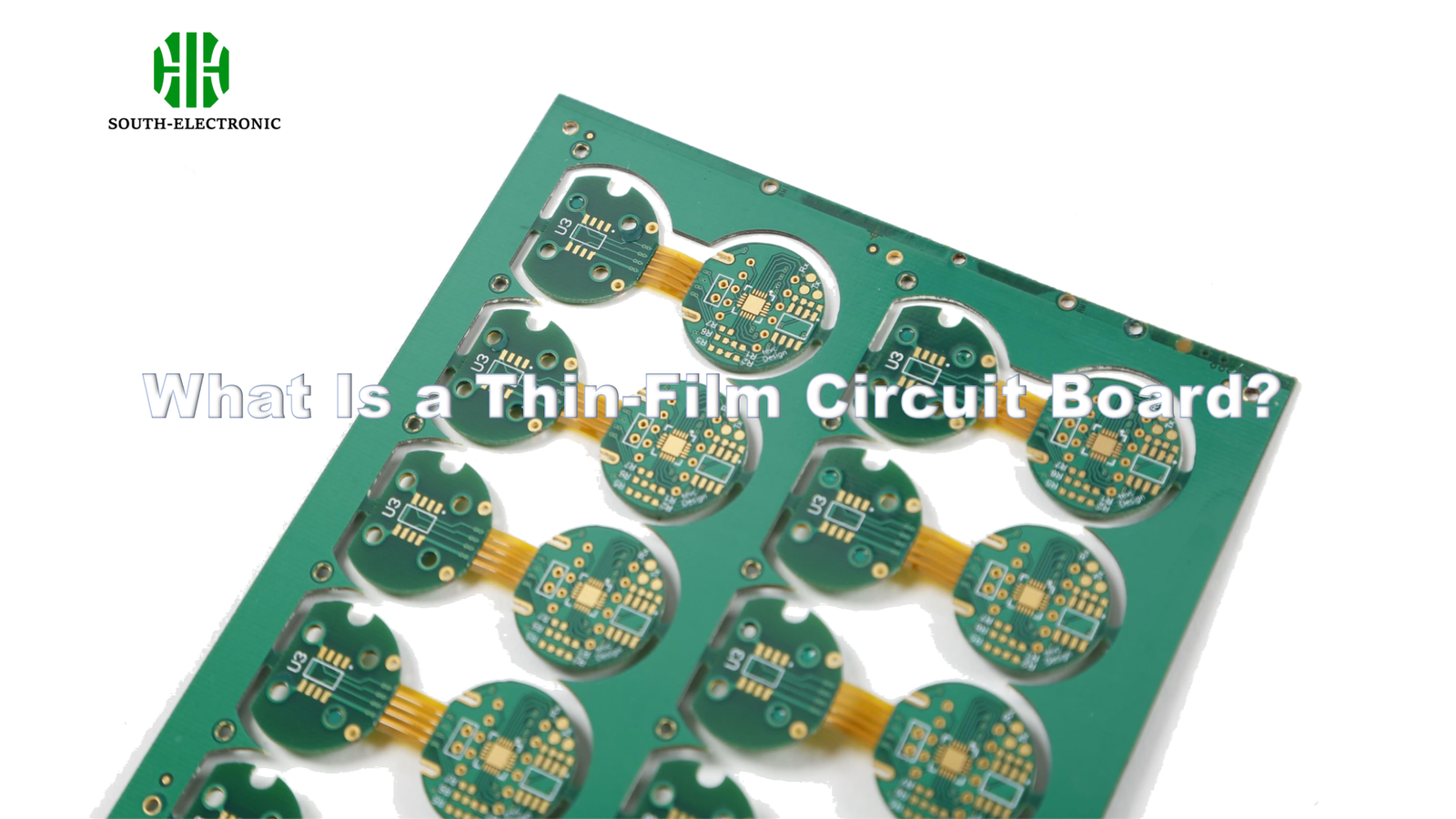
Thin-film circuit boards[^1] use micron-scale conductive layers[^2] (1-10μm) on ceramic substrates to achieve unmatched signal stability at ultra-high frequencies (>40 GHz). They power mission-critical systems where failure isn’t an option – from satellite communications to life-sustaining neurostimulators.
While traditional circuit boards struggle with modern demands, thin-film technology breaks through physical limits. Let’s dissect four revolutionary aspects redefining electronics as we know them.
How Do Thin-Film PCBs Achieve Superior Precision for Microelectronics?
Ever wondered how pacemakers contain entire cardiac monitoring systems? The secret is surgical-grade circuit precision[^3] that makes conventional PCBs look like blunt instruments.
Photolithographic patterning enables 10μm circuit features (vs. 100μm in standard PCBs), allowing 86% size reduction for implantable devices while maintaining 99.99% signal accuracy through controlled impedance matching.
)
Precision Engineering Breakdown
Three key manufacturing stages create this microscopic perfection:
| Process Stage | Thin-Film Method | Standard PCB Method | Precision Gain |
|---|---|---|---|
| Layer Deposition | Sputtered copper (0.5μm uniformity) | Electroplated copper (±5μm variation) | 10x tighter control |
| Etching | Laser ablation (5μm resolution) | Chemical bath (50μm resolution) | 90% finer details |
| Registration | Optical alignment (±1μm) | Mechanical alignment (±25μm) | 25x better accuracy |
This table explains why leading neurotech companies like Neuralink adopted thin-film for brain-machine interfaces requiring electrode spacing under 20μm.
What Industries Require Thin-Film Circuitry’s Ultra-High Frequency Performance?
When radar systems detect hypersonic missiles at 100km range, there’s no room for signal distortion. That’s where thin-film’s RF supremacy becomes non-negotiable.
Aerospace (satellite phased arrays), defense (electronic warfare systems), and 5G mmWave infrastructure (28-40GHz base stations) all depend on thin-film boards’ <0.01dB insertion loss at 40GHz – a 300% performance leap over FR-4 alternatives.
)
Frequency Frontier Applications
Critical implementations demanding thin-film's RF purity[^4]:
1. Phased Array Radars
- 64-element antenna arrays requiring phase synchronization within 0.5°
- Achieves 1.2° beam steering accuracy vs 4.5° with laminate PCBs
2. Quantum Computing Interconnects
- Superconducting circuits operating at 0.01K temperatures
- Ceramic substrates maintain dimensional stability where FR-4 would delaminate
3. Terahertz Imaging
- Medical scanners detecting early-stage tumors
- Low-loss tangent (<0.001) enables 0.5THz signal transmission
Why Choose Ceramic Substrates Over FR-4 in Advanced Thin-Film Boards?
Imagine circuit materials that laugh at soldering irons. Ceramic substrates handle 400°C thermal shocks that would fry conventional boards in seconds.
Aluminum nitride ceramics provide 170 W/mK thermal conductivity (470x better than FR-4) while matching silicon's CTE (4.5 ppm/°C). This prevents LED or power IC failure in extreme conditions.
)
Material Showdown: Ceramic vs FR-4
| Property | AlN Ceramic | FR-4 | Advantage Impact |
|---|---|---|---|
| Thermal Conductivity | 170 W/mK | 0.3 W/mK | 566x better heat dissipation |
| Dielectric Constant | 8.9 @10GHz | 4.5 @10GHz | Stable signal speed |
| CTE (ppm/°C) | 4.5 | 14 | 68% better component reliability |
| Max Temp | 450°C | 130°C | Enables harsh environment use |
| Cost/cm² | $0.85 | $0.03 | Justified for critical systems |
This explains Boeing's switch to ceramic thin-film boards in jet engine monitoring systems surviving 300°C operational temps.
Can Thin-Film Technology Solve Flexible Hybrid Electronics (FHE) Challenges?
Medical patches that conform to beating hearts while monitoring ECG? Thin-film's flexibility breakthrough makes this possible without circuit cracking.
Polyimide-based thin films achieve 0.1mm bending radius durability through 1μm ductile copper layers – enabling 500k flex cycles vs 50k in standard flex circuits. Vital for wearable dialysis machines and industrial strain sensors.
)
Hybrid Electronics Innovation Framework
| Challenge | Thin-Film Solution | Result |
|---|---|---|
| Component Warpage | Matched CTE substrates | 0.02mm placement accuracy after 1k thermal cycles |
| Dynamic Flexing | Elastic modulus <3GPa | Maintains conductivity at 40% tensile strain |
| High-Density IO | Embedded vias <15μm | 25% higher component density vs rigid-flex |
| Biocompatibility | USP Class VI materials | 5-year implantable devices approved by FDA |
Medtronic's latest glucose monitors leverage these advances for subcutaneous sensors with 180-day continuous operation.
Conclusion
When conventional circuits hit physical limits, thin-film technology delivers microscopic precision, extreme environment resilience, and groundbreaking flexibility – making the impossible routine in mission-critical electronics.
[^1]: Explore how thin-film circuit boards revolutionize electronics with unmatched signal stability and precision, crucial for advanced applications.
[^2]: Discover the impact of micron-scale conductive layers on electronic performance, enhancing efficiency and reliability in critical systems.
[^3]: Learn about surgical-grade circuit precision and its vital role in medical devices, ensuring safety and effectiveness in life-saving technologies.
[^4]: Learn about RF purity and its significance in thin-film circuitry, crucial for applications like radar and quantum computing.

