
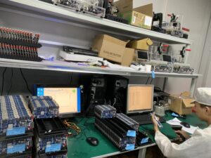
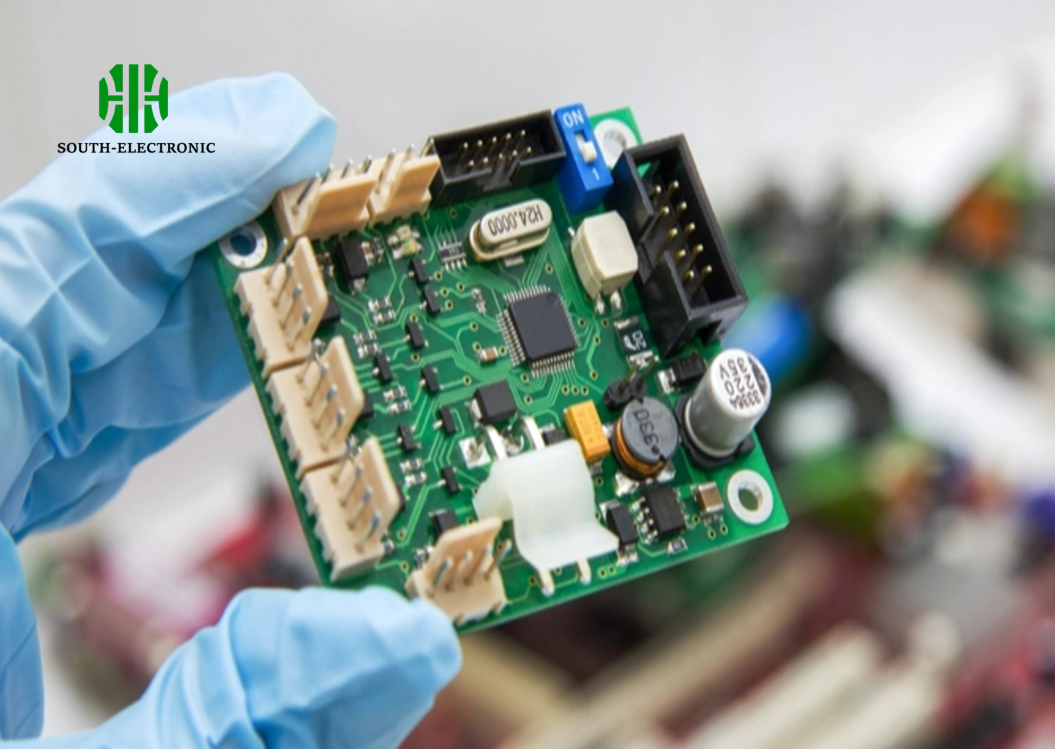
Through-Hole Assembly Supplier
South-Electronic
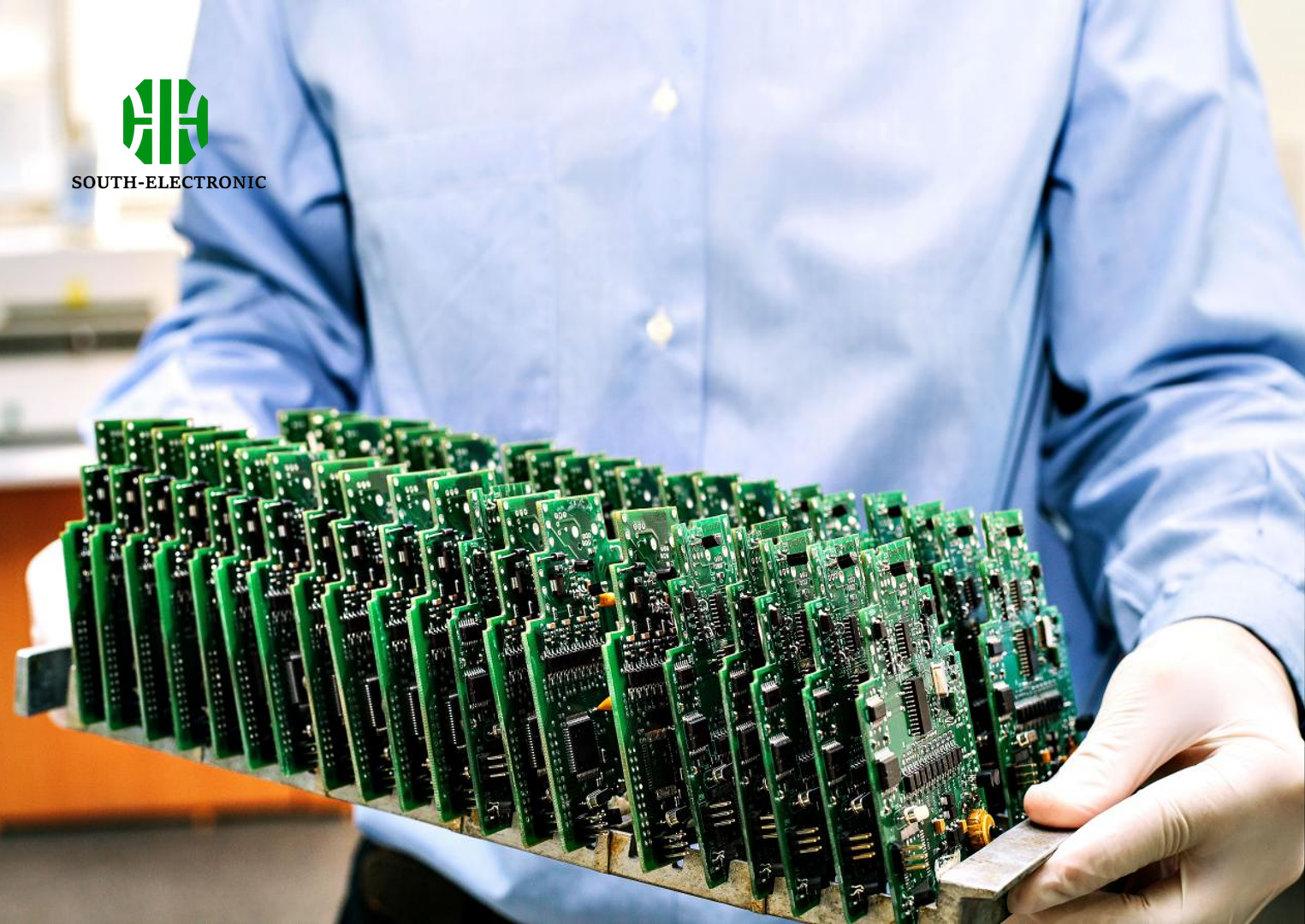
Look no further than South-Electronic for top-notch quality, reliability, and unbeatable value in your PCB assembly needs. See the difference with our all-in -one Through-Hole PCB Assembly service – from design to assembly, we guarantee accuracy, longevity, and compliance with the highest industry standards.
Your Trusted Supplier of Through-Hole PCB Assembly
Welcome to South-Electronic, where you’ll discover top-tier Through-Hole PCB Assembly services known for their excellent precision and reliability.
Whether you need single-layer, double-layer, or multi-layer boards, we tailor our services to enhance your electronic ventures, boost device performance, and guarantee exceptional value. Enjoy flexible ordering with as little as one piece, benefit from our expert team’s experience, and experience rapid delivery with our optimized production lines.
Why Choose South-Electronic?
-
Flexibility Ordering
You can order as few as 1 piece to fit your exact HDI needs.
Enjoy the flexibility to test new designs or meet small batch requirements without any hassle. -
Expert Team
You gain from our decade of industry expertise.
We understand your challenges and provide expert solutions and reliable support every step of the way. -
Comprehensive Service
You get complete satisfaction with our wide range of equipment.
Our comprehensive service ensures you get everything you need for a seamless experience. -
Fast Delivery
You benefit from our quick and efficient production times.
We prioritize timely delivery to meet your deadlines and keep your projects on track. -
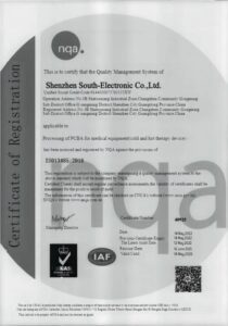
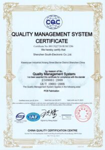
Guaranteed Satisfaction
You’re assured of quality and clear communication with our ISO9001 certification.
Your satisfaction is our priority, and we’re dedicated to exceeding your expectations with every order.
Related Project We had Done
Customer Reviews
Common Questions
Most Popular Questions
Send us a message
The more detailed you fill out, the faster we can move to the next step.


The Complete Guide For Through-Hole Assembly
Contents
Chapter 1
Introduction to Through-Hole Assembly
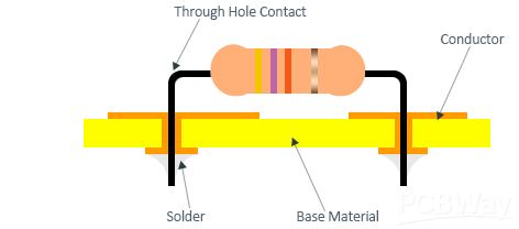
Through-hole technology is a classic method in the electronics manufacturing field. It involves mounting electronic components onto printed circuit boards (PCBs) by inserting their leads through holes drilled in the board. This traditional technique was the mainstay of electronics assembly before the advent of more modern methods like surface-mount technology (SMT).
In through-hole assembly, once the component leads are inserted through the holes, they are soldered to pads on the opposite side of the board. This creates a strong mechanical connection that also serves as the electrical link between the components and the PCB. This method is known for its reliability and durability, making it a preferred choice in applications where mechanical stress or environmental factors, such as heat or vibrations, are concerns.
Importance and Advantages in Electronics Manufacturing
Through-hole technology continues to play a significant role in certain manufacturing scenarios despite advances in other assembly techniques. Here are some key advantages:
- Mechanical Strength: The lead-through-the-hole method offers superior mechanical bonds compared to surface mounting. This makes it ideal for components that may be subject to mechanical stresses or need strong physical support, such as connectors or heavy components.
- Ease of Prototyping and Testing: Through-hole components are often easier to handle and manipulate during prototyping and testing phases, allowing for easier modifications and adjustments.
- Environmental Resilience: Due to the robust solder joints, through-hole assemblies are more resistant to environmental factors, such as shock and vibration. This makes them suitable for aerospace, military, and automotive industries where such conditions are prevalent.
- Power Handling: Components that dissipate more power or require higher current handling capabilities are better suited for through-hole assembly due to the larger contact areas provided by the leads.
Comparative Introduction to Surface-Mount Technology (SMT)
While through-hole technology was once the standard in electronics assembly, the development of surface-mount technology (SMT) has provided a compact and efficient alternative. Unlike through-hole assembly, SMT components are mounted directly onto the surface of the PCB without drilling holes, which allows for smaller PCB designs and higher component density.
Comparison Highlights:
- Size and Weight: SMT allows for more compact designs as it eliminates the need for holes and uses smaller components, making it ideal for modern, miniaturized consumer electronics like smartphones and laptops.
- Assembly Speed: SMT enables faster, automated assembly processes as it simplifies the component placement phase, allowing for high-volume production with minimal manual intervention.
- Cost Efficiency: The ability to automate more processes and the reduced material costs due to smaller component sizes often lead to cost efficiencies in SMT.
However, through-hole technology remains indispensable for specific applications where durability, testing flexibility, and power handling are priorities. Therefore, many modern electronics assemblies utilize a combination of both techniques, each serving its distinct role in the final product design. Through this blend, manufacturers leverage the strengths of both methodologies to produce robust, efficient electronics that meet diverse application requirements.
Chapter 2
History and Evolution of Through-Hole Technology
Historical Context and Development
The inception of through-hole technology dates back to the mid-20th century, coinciding with the rapid growth of the electronics industry. As electronic devices evolved in complexity throughout the 1950s and 1960s, there arose a pressing need for a reliable method to firmly attach electronic components to circuit boards. This led to the development and widespread adoption of through-hole technology.
Initially, electronic circuits were constructed using point-to-point wiring, which was labor-intensive and prone to errors. The introduction of the printed circuit board (PCB) revolutionized this process. With PCBs, components could be soldered onto a board pre-printed with conductive pathways, streamlining assembly and significantly improving reliability.
Through-hole technology became the standard during this era for several reasons:
- Reliability: The soldering of component leads through drilled holes provided a robust electrical and mechanical connection, crucial for the dependability of electronic devices.
- Ease of Prototyping: The ability to insert and replace components easily facilitated prototyping and testing, which spurred rapid innovation and product development.
Transition from Early Electronics to Modern Applications
As technology advanced and demand increased for more compact and efficient electronic devices, assembly methods evolved. By the late 20th century, surface-mount technology (SMT) emerged, offering considerable advantages in terms of size reduction and manufacturing efficiency. However, through-hole technology persisted—particularly in applications that required greater mechanical strength and component durability.
Today’s electronics integrate both through-hole and SMT to capitalize on the benefits of each:
Modern Applications: Through-hole technology is still actively employed in the production of high-stress or power-critical components, such as connectors, transformers, and large capacitors. Its durability remains unmatched in applications subjected to mechanical strain or extreme environments, such as military or aerospace technologies.
Combined Approach: Many contemporary electronics utilize a mixed assembly approach, leveraging both SMT for miniaturization and through-hole for strength, thereby optimizing product performance. This hybridization allows for innovation in complex devices like automotive control systems, industrial machinery, and sophisticated consumer electronics.
Legacy and Future: Despite the rise of SMT, through-hole technology’s legacy endures as it continues to provide unmatched reliability in critical applications. The ongoing evolution of this technology demonstrates its adaptability, ensuring its relevance in an ever-changing industry, sustaining its fundamental role in the electronics assembly landscape for decades to come.
Chapter 3
Components Used in Through-Hole Assembly
Types of Components
Through-hole assembly primarily involves components known for their leaded form, where the component leads or pins are inserted through drilled holes on a PCB. Here are some common types of components used in through-hole technology:
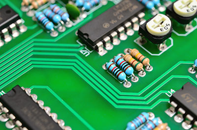
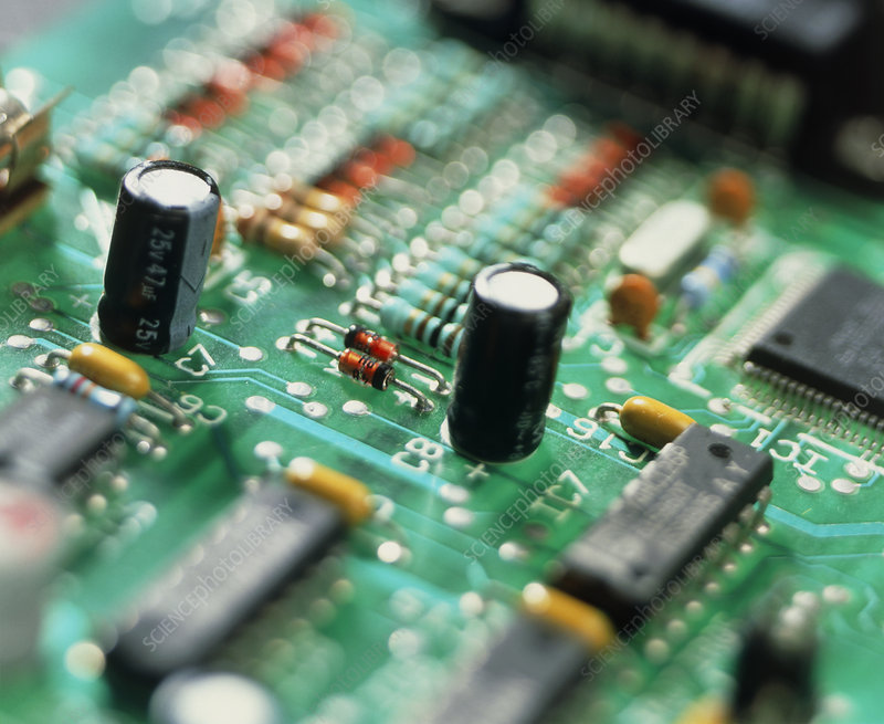
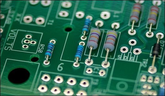
Resistors: These components control the flow of electrical current within circuits. They are typically cylindrical with axial leads extending from both ends, known as leaded resistors.
Capacitors: Used for storing and releasing electrical energy, capacitors in through-hole form are often either radial or axial. Radial capacitors have two leads coming out of one end, making them compact, whereas axial capacitors have leads extending from each end.
Diodes: These components allow current to flow in one direction only, acting as a check valve for electricity. Diodes, like rectifiers and LEDs, are commonly found with leads for through-hole insertion.
Transistors: Used to amplify and switch electronic signals, transistors in through-hole form usually come as single, vertically standing devices with three leads.
Inductors: Like small coils, these components store energy in a magnetic field when current passes through. Leaded inductors are often used where higher power handling is needed.
Integrated Circuits (ICs): These can range from simple gates to complex processors, usually in a dual in-line package (DIP) format for through-hole mounting, offering higher power dissipation compared to their SMT counterparts.
Connectors: Essential for linking different parts of a system, through-hole connectors provide sturdy mechanical stability and are capable of handling significant environmental and physical stress.
Detailed Explanation of Leaded Components versus SMT Components
The key distinction between leaded (through-hole) components and SMT components lies in their design and application:
Leaded Components: These components are characterized by their wire leads, which extend from the body of the component through holes in the PCB. This method enables them to form stronger mechanical connections, making them suitable for applications where durability is essential. The larger size of leaded components facilitates easier manual handling during assembly and testing, especially useful in prototypes and low-volume manufacturing.
SMT Components: In contrast, SMT components are designed to be placed directly onto the surface of the PCB without the need for through-holes. This allows for increased circuit density and reduced board space, crucial for modern electronics that demand compact design. SMT leads are typically shorter and flatter, facilitating automated assembly but often making manual repair more challenging.
Benefits Distinction:
- Mechanical Stability: Leaded components excel in applications where components need to withstand mechanical stress, shock, and vibration.
- Space Efficiency: SMT components are ideal for devices requiring high component density and miniaturization.
Both types play integral roles in modern electronics. Through-hole components offer reliability and robustness where needed, while SMT components provide compact size and lower production costs, enabling manufacturers to meet diverse technological demands efficiently and effectively. The choice between the two often depends on specific application requirements, manufacturing capabilities, and product design goals.
Chapter 4
The Through-Hole Assembly Process
The through-hole assembly process is a meticulous procedure that ensures components are securely and reliably attached to a printed circuit board (PCB). This process involves several critical steps, each playing a vital role in the quality and functionality of the final product. Here’s a step-by-step breakdown of the through-hole assembly process:
Step-by-Step Breakdown of the Assembly Process
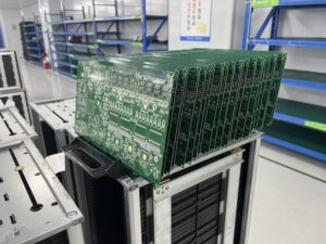
Preparation and PCB Fabrication
- Begin with the design and fabrication of the PCB according to the specific circuit design. This involves creating the board with pre-drilled holes to accommodate component leads and printed conductive paths for electrical connections.
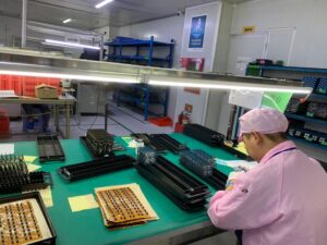
Component Sorting and Preparation
- Components are sorted and prepared as per the circuit design requirements. This includes gathering resistors, capacitors, diodes, and other lead-based components needed for assembly.
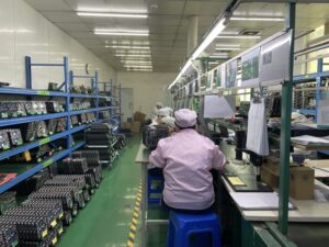
Component Insertion
- Skilled technicians manually insert the leads of each component into the designated holes on the PCB. This process requires precision to ensure that each component is placed correctly to match the circuit layout.
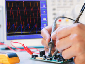
Soldering Techniques
- Once components are placed, the board undergoes a soldering process to create a reliable electrical and mechanical connection. There are two primary soldering techniques used:
a. Wave Soldering: For large-scale production, PCBs are passed over a wave of molten solder. The solder adheres to the exposed metal areas and component leads, forming joints as it cools.
b. Manual Soldering: For smaller quantities or delicate components, technicians use soldering irons to hand-solder each connection individually, allowing for precision and control.
Trimming of Excess Leads
- After soldering, any protruding component leads are trimmed to prevent short circuits and interference with other parts of the device.
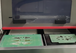
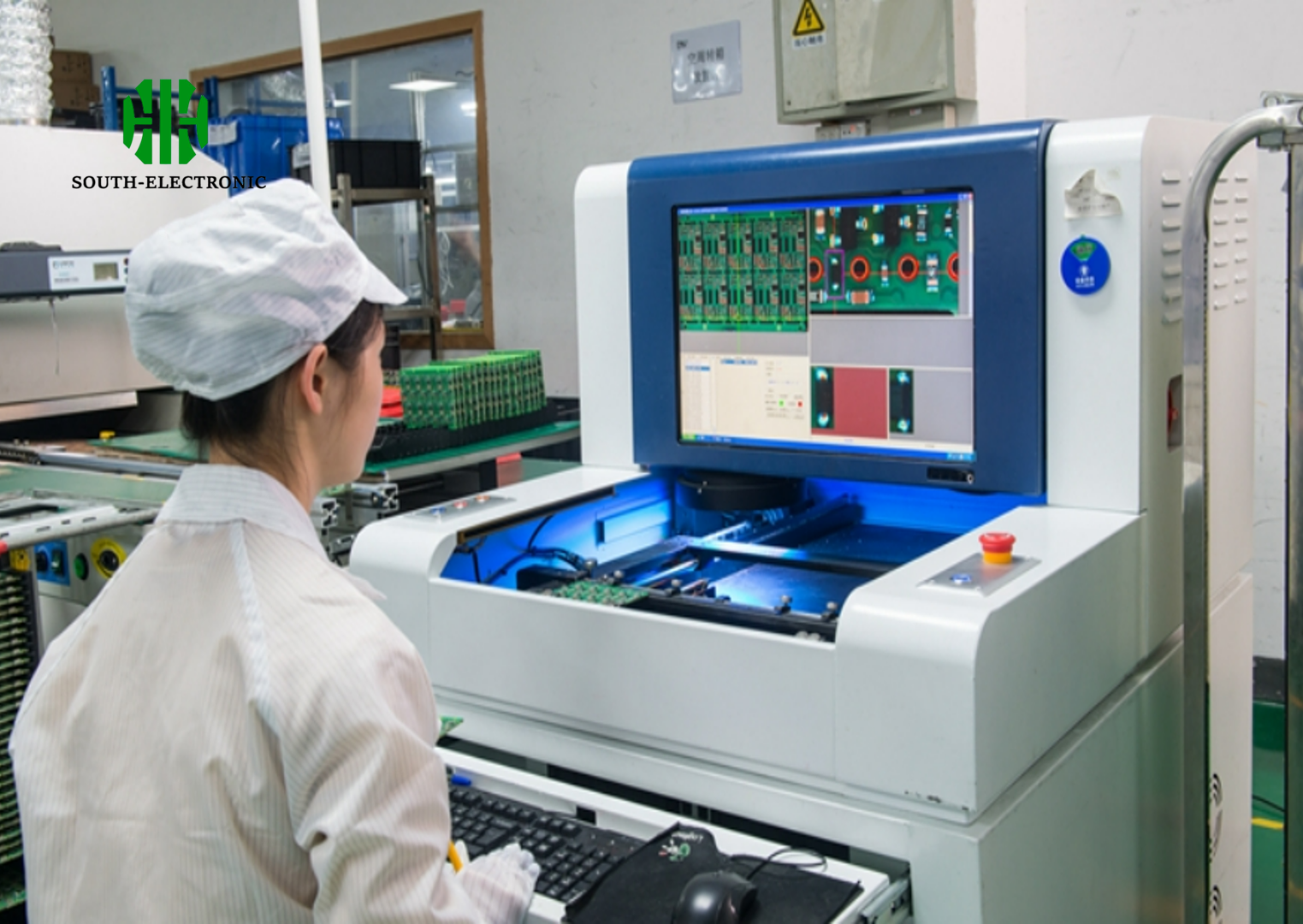
Inspection and Quality Control
- The assembled boards undergo rigorous inspection processes to ensure all components are correctly placed and securely soldered. This includes visual checks and automated optical inspections (AOI) to detect any soldering defects or placement errors.
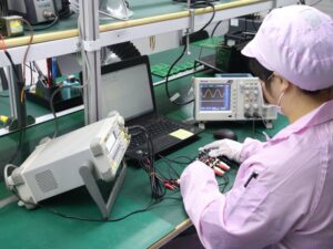
Functional Testing
- Completed assemblies are subjected to electrical tests to verify that the circuit functions as intended. This can involve power tests, signal integrity checks, and other diagnostic measures to identify any potential issues.
Repair and Rework (if necessary)
- Any detected defects during inspection and testing are addressed through repair and rework processes. This may include re-soldering connections, replacing faulty components, or other corrective measures.
Final Assembly and Packaging
- Once all components are correctly assembled and tested, the PCB may be enclosed within a housing or case, integrating it into the final product design. The final assembled products are then packaged for shipment and distribution.
In-Depth Look at Component Insertion, Soldering Techniques, and Inspection
Component Insertion: This step is fundamental as it determines the subsequent processes. Accuracy and consistency in placing each component ensure efficient soldering and minimize post-soldering issues.
Soldering Techniques: Wave soldering is efficient for mass production, ensuring uniform solder application across multiple boards. Manual soldering, however, allows for meticulous craftsmanship, essential for prototyping and detailed work.
Inspection: Quality control is integrated into various stages of assembly. Inspections not only ensure compliance with design specifications but also help in maintaining the reliability and safety of the electronic product. Techniques like AOI and in-circuit testing (ICT) are often employed to enhance inspection accuracy.
Through these systematic processes, through-hole assembly delivers robust and dependable electronic connections, ensuring operational excellence and longevity in a wide array of electronic products.
Chapter 5
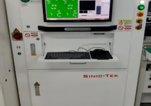
Equipment and Tools for Through-Hole Assembly
The through-hole assembly process relies on a diverse array of equipment and tools to ensure the effective and efficient attachment of electronic components to printed circuit boards (PCBs). Here, we explore the essential tools traditionally used in through-hole assembly, and highlight the latest technologies transforming these processes.
Overview of Essential Tools
Soldering Stations:
- These are fundamental in through-hole assembly, especially for manual soldering. Soldering stations typically consist of a soldering iron, a stand, and temperature controls, allowing operators to handle delicate components with precision and consistent heat application.
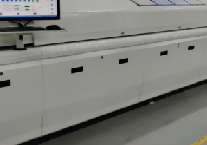
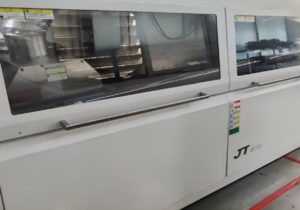
Wave Solder Machines:
- Essential for high-volume production, wave solder machines automate the soldering process by creating a wave of molten solder. PCBs are conveyed over this wave, securely soldering all through-hole components in one swift motion, greatly enhancing productivity and uniformity.
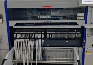
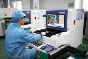
Component Insertion Machines:
- Although many through-hole components are placed manually, automated insertion machines can be employed for certain applications. These machines provide speed and accuracy in placing components, thereby reducing human error.
Desoldering Tools:
- Desoldering stations and pumps are used to remove solder from components and PCBs, which is crucial during repair or rework processes. These tools help in efficiently disengaging components without damaging the board.
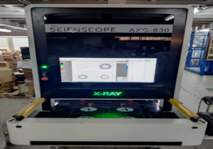
Inspection Tools:
- Magnifying lamps, microscopes, and Automated Optical Inspection (AOI) systems are indispensable for verifying solder joints and component placement. These tools ensure that assembly meets the necessary standards and specifications.
Cutting Instruments:
- Lead cutters are used to trim excess component leads post-soldering, aiding in the prevention of shorts and interference with the PCB.
Latest Technologies Transforming Assembly Processes
Automated Soldering Technologies:
- Advanced robotic soldering machines offer precision and repeatability far exceeding manual soldering capabilities. These robots can be programmed for specific tasks, optimizing throughput and ensuring consistent quality across complex assemblies.
Precision Laser Soldering:
- Utilized for delicate or high-precision applications, laser soldering provides focused heat application, minimizing thermal stress on components and allowing for precise control in soldering delicate leads.
Smart Inspection Systems:
- AI-driven inspection technologies are increasingly being integrated into assembly lines. These systems leverage machine learning to identify defects with greater accuracy and speed than traditional inspection methods, providing real-time insights and rapid feedback.
Environmental Control Systems:
- Innovations in ESD (Electrostatic Discharge) protective equipment and climate control systems enhance the operating environment, ensuring the high reliability of soldering processes by minimizing environmental impacts and enhancing operator safety.
Advanced Reflow Ovens:
- Though primarily used in SMT, advanced reflow technologies are sometimes applied in hybrid assembly environments. Integration with through-hole can occur in mixed-technology board designs, reflecting flexibility in assembly lines.
These advancements illustrate the ongoing evolution of equipment and tools in through-hole assembly, ensuring that this dependable assembly method adapts to modern demands for speed, precision, and quality in electronics manufacturing. Through the integration of cutting-edge technologies, manufacturers continue to enhance the reliability and efficiency of through-hole processes, keeping pace with the dynamic changes in the electronics industry.
Chapter 6
Design Considerations for Through-Hole Assemblies
Designing printed circuit boards (PCBs) for through-hole assembly requires particular attention to detail and adherence to specific guidelines that account for the characteristics of through-hole technology. These considerations ensure that the final product is both manufacturable and reliable, capable of meeting the demands of its intended application. Below are the key guidelines and tips to optimize design for through-hole assemblies.
PCB Design Guidelines Specific to Through-Hole Technology
Hole and Pad Sizing:
- Drill Sizes: Carefully select drill sizes that accommodate the component leads with adequate clearance. A general rule is to have hole diameters that are 0.1mm to 0.2mm larger than the lead diameter to facilitate easy insertion and soldering.
- Pad Sizes: Ensure that pads are sufficiently large to enable a good solder joint. This typically means the pad diameter should be at least 1.5 times the hole diameter, providing enough surface area for effective solder adhesion.
Trace and Space Rules:
- Current Carrying Capacity: Design traces to be wide enough to carry the necessary current without overheating. Use PCB trace width calculators to determine the appropriate dimensions based on current requirements and voltage drop considerations.
- Spacing: Maintain proper spacing between pads and traces to prevent short circuits and to account for solder bridging, particularly in areas with high component density.
Component Layout and Orientation:
- Logical Placement: Group related components together logically to minimize trace lengths and improve signal integrity.
- Orientation: Align components such that their polarized leads (like cathodes on diodes) are consistently oriented. This simplifies the assembly process and reduces the risk of orientation errors.
Layer Considerations:
- Multi-layer Boards: Though through-hole components are often on double-sided boards, consider additional layers for ground planes and power distribution, which help reduce EMI and improve signal performance.
Thermal Management:
- Heat Sinks and Vias: Incorporate heat sinks or thermal vias in your design for components that dissipate substantial heat, ensuring that your design effectively manages thermal loads.
Tips for Optimizing Design for Manufacturability and Reliability
Standardize Components:
- Use standardized component sizes and footprints wherever possible to simplify procurement and reduce the likelihood of errors during component insertion and soldering.
Design for Testability:
- Include test points for critical signals at strategic locations on the board. This facilitates easier testing and troubleshooting during both the manufacturing process and subsequent maintenance.
Address Assembly Constraints:
- Lead Lengths: Design for the appropriate lead lengths to balance ease of insertion with mechanical stability. Leads should extend adequately through the board but not excessively beyond the underside.
- Component Clearance: Ensure there is sufficient clearance between components for assembly tools and handling, considering the physical size and orientation of tools used in soldering.
Durability Enhancements:
- Plated-Through Holes: Use plated-through holes to improve connection durability and to enhance electrical continuity between layers.
- Reinforced Board Areas: For boards subject to mechanical stress, consider reinforcing areas around components with higher mechanical load through additional padding or strategic placement of vias.
Documented Design and Assembly Instructions:
- Provide detailed design documentation and assembly instructions, including diagrams and orientation guides, to support consistency and reduce errors during the assembly process.
By focusing on these design considerations and guidelines, engineers and designers can create robust through-hole assemblies that offer durability, ease of manufacturing, and high reliability. These strategies support the creation of products well-suited for environments where through-hole technology remains the optimal choice, ensuring long-lasting performance and operational integrity.
Chapter 7

Advantages and Disadvantages of Through-Hole Assembly
Through-hole assembly is a time-tested method for mounting electronic components on a printed circuit board (PCB). While it has been partially supplanted by Surface Mount Technology (SMT) in many applications, through-hole assembly still holds distinct advantages in specific scenarios. Here, we provide a comprehensive comparison with SMT and outline the scenarios where through-hole assembly is preferable.
Advantages of Through-Hole Assembly
Mechanical Strength and Durability:
- Sturdy Connections: The leads of through-hole components extend through the PCB, creating a strong mechanical bond that is highly resistant to physical stress, vibration, and environmental factors. This makes through-hole assemblies ideal for applications in rugged environments.
Ease of Prototyping and Testing:
- Simple Manual Handling: Through-hole components are larger and easier to handle, which simplifies manual insertion and soldering during prototyping. This ease of use makes it quicker to build and test prototypes with through-hole components.
Reliability in High-Power Applications:
- Enhanced Thermal Performance: Through-hole components generally offer better heat dissipation due to their larger size and robust connections, making them suitable for high-power and high-voltage applications.
Facilitates High-Quality Solder Joints:
- Consistency: The straightforward nature of soldering leads through the board often results in higher-quality solder joints compared to SMT, where components rest on the surface of the PCB.
Disadvantages of Through-Hole Assembly
Board Space and Density:
- Less Compact: Through-hole components require more space on the PCB, limiting the component density and making them unsuitable for products where miniaturization is a priority.
Longer Assembly Time:
- Manual Processes: The manual nature of inserting components and soldering can increase production time and labor costs compared to the automated processes used in SMT.
Limited Applicability in Modern Electronics:
- Not Suitable for Small Components: Many modern electronic applications use very small components that are not available in through-hole form, necessitating SMT for such assemblies.
Comprehensive Comparison with SMT
Automated vs. Manual: SMT is well-suited to automated assembly processes, reducing labor costs and increasing production speed. Through-hole assembly, on the other hand, often relies on manual placement and soldering, which can be slower but may offer flexibility in prototyping and repair.
Durability vs. Miniaturization: SMT excels in applications where miniaturization and packing density are crucial, such as in smartphones and tablets. Through-hole assembly remains advantageous where durability and strong mechanical connections are required, such as in automotive, aerospace, and industrial applications.
Scenarios Where Through-Hole Assembly is Preferable
High-Reliability Applications:
- Aerospace and Defense: These sectors often require high-reliability connectors and components that maintain performance under extreme conditions, a scenario where the robustness of through-hole assembly is advantageous.
Large and Heavy Components:
- Transformers and Inductors: Large, heavy components benefit from the mechanical stability provided by through-hole assembly, ensuring secure mounting within the product housing.
Prototyping and Development:
- Ease of Modification: The simplicity of swapping out through-hole components for testing makes them ideal for prototype development where frequent changes and testing are required.
High-Voltage and High-Power Applications:
- Power Supplies and Converters: Through-hole components can better handle the size, thermal stress, and electrical demands typical of high-power applications.
Repair and Maintenance:
- Ease of Repair: The larger size and robust nature of through-hole components make them easier to remove and replace during maintenance or repair.
In conclusion, while through-hole assembly has been largely overtaken by SMT in consumer electronics due to the need for compact designs and automated production, it remains a vital technology in many niche and demanding applications where peak reliability and mechanical strength are non-negotiable. Understanding the inherent strengths of through-hole assembly helps designers and engineers select the most suitable technology for their specific application needs.
Chapter 8
Desafíos comunes en la montaje por agujeros
El montaje por agujeros, a pesar de sus ventajas en durabilidad y alta confiabilidad, presenta varios desafíos de fabricación. Estos desafíos pueden afectar la calidad, la eficiencia y la rentabilidad del proceso de montaje si no se abordan adecuadamente. A continuación, se presentan algunos problemas típicos que surgen durante la fabricación por agujeros y se ofrecen soluciones y mejores prácticas para mitigar estos errores comunes.
Problemas típicos que se enfrentan durante la fabricación
Mala alineación de componentes:
- Problema: Los componentes pueden estar mal alineados durante la inserción manual, lo que lleva a defectos de soldadura o fallos funcionales.
- Impacto: Los componentes mal alineados pueden causar problemas de conectividad eléctrica y afectar el rendimiento del producto final.
Mala formación de uniones de soldadura:
- Problema: La falta de soldadura, las temperaturas incorrectas o los ajustes incorrectos de la ola de soldadura pueden resultar en uniones de soldadura deficientes.
- Impacto: Las uniones de soldadura débiles pueden causar conexiones intermitentes o fallos de circuito completos.
Puente de soldadura excesivo:
- Problema: Cuando los componentes están demasiado cerca entre sí o la soldadura es inexacta, se pueden formar puentes de soldadura entre conexiones adyacentes.
- Impacto: Esto puede llevar a cortocircuitos y potencialmente dañar la placa o los componentes.
Problemas de integridad de pads y agujeros:
- Problema: La perforación incorrecta, el revestimiento deficiente o el calor excesivo pueden dañar los pads y los agujeros en la placa de circuito impreso (PCB).
- Impacto: Los pads y agujeros dañados pueden resultar en conexiones mecánicas deficientes y trayectorias eléctricas no confiables.
Daño de componentes por calor:
- Problema: Los componentes sensibles al calor pueden dañarse durante los procesos de soldadura, afectando su funcionalidad.
- Impacto: Los componentes dañados pueden llevar a fallos en el circuito y necesitar rework o reemplazo costoso.
Inconsistencias en la soldadura por ola:
- Problema: Las variaciones en las condiciones de soldadura por ola pueden llevar a una cobertura de soldadura inconsistente y problemas de calidad en toda la placa.
- Impacto: Resulta en una calidad de producto variable, necesitando inspección y rework aumentados.
Soluciones y mejores prácticas para evitar errores comunes
Colocación precisa de componentes:
- Solución: Utilice guías de inserción de componentes y máquinas de inserción automatizadas cuando sea posible para garantizar una colocación precisa. La marcación clara de la orientación de los componentes en las PCB puede ayudar en las inserciones manuales.
- Mejor práctica: Capacite a los técnicos de montaje rigurosamente en técnicas de colocación y en la importancia de mantener la alineación.
Optimización de procesos de soldadura:
- Solución: Monitoree y controle cuidadosamente las temperaturas y duraciones de soldadura para garantizar un flujo óptimo de soldadura y resistencia de la unión.
- Mejor práctica: Implemente un régimen de control de proceso sólido para las máquinas de soldadura por ola, verificando rutinariamente la consistencia de la temperatura y el mantenimiento del nivel de soldadura.
Gestión del puente de soldadura:
- Solución: Asegúrese de que haya un espacio adecuado entre los componentes y utilice máscaras de soldadura para minimizar los riesgos de puente. Ajuste los parámetros de la soldadura por ola para controlar la profundidad y la dispersión del depósito de soldadura.
- Mejor práctica: Diseñe placas con un mayor espaciado entre pads cuando sea posible y realice pruebas regulares de puentes de soldadura durante las corridas de producción.
Garantizar la calidad de pads y agujeros:
- Solución: Utilice procesos de fabricación de PCB precisos y confiables para mantener la calidad de los agujeros y pads. Emplee una inspección de calidad para verificar defectos como la perforación insuficiente o la delaminación.
- Mejor práctica: Incorpore controles de calidad estrictos en el proceso de fabricación de PCB, incluyendo auditorías y verificaciones regulares en etapas clave de producción.
Gestión del calor:
- Solución: Emplee fases de precalentamiento antes de la soldadura para minimizar el choque térmico, y seleccione soldaduras con puntos de fusión adecuados para componentes delicados.
- Mejor práctica: Diseñe placas que incluyan alivios térmicos o disipadores de calor para componentes particularmente sensibles al calor. Revise regularmente los perfiles de soldadura para adaptarse a nuevos componentes.
Soldadura por ola consistente:
- Solución: Calibre y mantenga regularmente el equipo de soldadura por ola para garantizar una altura y temperatura de ola consistentes.
- Mejor práctica: Realice verificaciones de calibración y actividades de mantenimiento rutinarias para las máquinas de soldadura por ola y mantenga registros detallados para identificar y abordar las fluctuaciones de manera oportuna.
Al entender y prepararse para estos desafíos comunes, los fabricantes no solo pueden mejorar la calidad y la confiabilidad de los montajes por agujeros, sino también aumentar la eficiencia y reducir los costos de fabricación. La implementación de mejores prácticas y soluciones como parte de los procedimientos operativos estándar garantizará un proceso de fabricación sólido capaz de entregar montajes por agujeros de alta calidad una y otra vez.
Chapter 9
Quality Assurance and Testing in Through-Hole Assemblies
Ensuring quality in through-hole assemblies is crucial for maintaining the reliability and performance of electronic products. Quality assurance encompasses a wide range of methodologies and testing techniques designed to identify and rectify potential issues throughout the manufacturing process. Here, we delve into effective methods for quality assurance and highlight key testing techniques such as in-circuit testing (ICT) and functional testing.
Methods for Ensuring Quality in Through-Hole Assemblies
Robust Design Review:
- Design Validation: Conduct thorough design reviews to ensure that PCB designs adhere to best practices for through-hole assembly. This includes verifying component footprints, hole sizes, and layout considerations.
- Simulation and Analysis: Utilize simulation tools to anticipate potential issues such as thermal stresses and solder joint reliability before entering the production phase.
Process Control:
- Standardized Procedures: Implement standardized assembly procedures to minimize variability in processes such as component placement and soldering.
- Continuous Monitoring: Employ sensors and monitoring tools to continuously track key parameters during assembly, such as solder temperature and wave solder level.
Materials Inspection:
- Component Verification: Inspect incoming components for compliance with specifications, checking for defects or damage that could affect assembly quality.
- Solder and Material Quality: Ensure the quality of solders and other materials by sourcing from reliable suppliers and conducting regular material quality audits.
Operator Training:
- Skill Development: Provide comprehensive training programs for assembly line workers to ensure proficient handling of through-hole components and adherence to quality procedures.
- Certification and Recertification: Certify operators in key processes and conduct regular recertification to keep skills current and align with industry standards.
Testing Techniques for Through-Hole Assemblies
In-Circuit Testing (ICT):
- Purpose: ICT is used to verify the electrical performance and connections within a circuit. It checks for shorts, opens, resistance, capacitance, and other parameters directly on the board.
- Method: Utilizes a bed of nails fixture to access test points on the PCB, allowing for comprehensive testing of each node in the circuit.
- Advantages: Provides fast, accurate feedback on assembly defects such as incorrect component values, solder joint issues, and other assembly errors, enabling rapid identification and correction.
Functional Testing:
- Purpose: Functional testing evaluates the PCB’s performance under real-world conditions, ensuring that the entire assembly functions according to the design’s specifications.
- Method: Boards are connected to a test system that simulates their operating environment, assessing how well the assembled PCB performs its intended function.
- Advantages: Verifies that the final product will function as intended in the end application, providing assurance that components interact correctly and that the system achieves the desired performance levels.
Visual Inspection:
- Purpose: To visually verify the placement and solder quality of components on the PCB, detecting obvious assembly issues before functional testing.
- Method: Performed manually by trained inspectors or using automated optical inspection (AOI) systems to quickly and accurately assess the board.
- Advantages: Allows early detection of misaligned components, insufficient solder, and other visual defects, reducing the need for rework.
Environmental and Stress Testing:
- Purpose: To assess how the assembled product performs under various environmental conditions such as temperature extremes, humidity, and physical shock.
- Method: Expose boards to conditions that simulate real-world stresses and measure their ability to withstand these without degradation in performance or reliability.
- Advantages: Ensures that the product will maintain functionality and reliability under diverse operating conditions, crucial for high-stress applications like automotive and aerospace.
By employing these quality assurance methods and testing techniques, manufacturers can ensure that through-hole assemblies meet stringent quality standards. This comprehensive approach not only enhances the reliability and functionality of electronic products but also mitigates risks associated with assembly defects, thereby supporting long-term customer satisfaction and brand reputation.
Chapter 10
Future Trends and Innovations in Through-Hole Assembly
As the electronics industry continues to evolve, through-hole assembly is poised to undergo significant advancements driven by emerging technologies and innovative methods. These future trends not only promise to enhance the efficiency and quality of through-hole assemblies but also offer novel solutions to longstanding challenges. Below, we explore upcoming trends and how they might reshape the landscape of through-hole assembly.
Automation and Robotics:
- Advanced Automation: The integration of sophisticated robotics and automation solutions in through-hole assembly lines is set to increase precision and speed. Automated component insertion and soldering robots can minimize human errors and improve consistency in assembly processes.
- Collaborative Robots (Cobots): Cobots are designed to work alongside human operators, providing assistance in complex tasks that require a combination of machine precision and human intuition. This hybrid approach can significantly enhance productivity and quality.
3D Printing and Additive Manufacturing:
- Component Fabrication: As 3D printing technology advances, it has the potential to revolutionize the way components are manufactured and integrated into through-hole assemblies, particularly for custom or low-volume production runs.
- Prototype Development: Additive manufacturing can expedite prototyping processes, allowing designers to rapidly test and refine through-hole designs before full-scale production.
Advanced Materials and Coatings:
- High-Performance Alloys: The development of new metal alloys and coatings can improve thermal and electrical performance, making through-hole components more robust and reliable.
- Environmental Coatings: Innovations in protective coatings can enhance the durability of through-hole assemblies against environmental factors such as moisture, heat, and corrosion.
Integration of IoT and AI:
- Smart Manufacturing: Internet of Things (IoT) devices can be used to monitor and control various aspects of the assembly process in real-time, providing detailed analytics and insights that can drive improvements in efficiency and quality.
- AI-Driven Quality Control: Artificial intelligence can be employed to analyze data from testing and inspection processes, identifying patterns and predicting potential defects before they manifest, thus enabling preemptive corrective actions.
Get in touch
Where Are We?
Industrial Park, No. 438 Donghuan Road, No. 438, Shajing Donghuan Road, Bao'an District, Shenzhen, Guangdong, China
Floor 4, Zhihui Creative Building, No.2005 Xihuan Road, Shajing, Baoan District, Shenzhen, China
ROOM A1-13,FLOOR 3,YEE LIM INDUSTRIAL CENTRE 2-28 KWAI LOK STREET, KWAI CHUNG HK
service@southelectronicpcb.com
Phone : +86 400 878 3488
Send us a message
The more detailed you fill out, the faster we can move to the next step.

