
High-speed PCB design is a crucial aspect of modern electronics, where signal integrity and performance are paramount. Ensuring your PCB can handle high-speed signals without issues requires meticulous planning and implementation of best practices. Below, we explore 11 essential high-speed PCB routing practices that can significantly improve your PCB design’s performance and reliability.
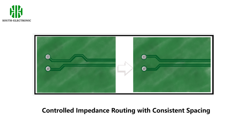
Tip 1: Controlled Impedance Routing with Consistent Spacing
Controlled impedance is a big deal for high-speed signal integrity. It means you have to keep the trace width and spacing the same so the impedance of the trace matches what you designed. If you don’t, you’ll get signal reflections, which can corrupt or lose your data. Implementation Tip: Use simulation tools to figure out what trace width and spacing you need. Don’t forget to consider the dielectric constant of the PCB material because it affects the impedance.
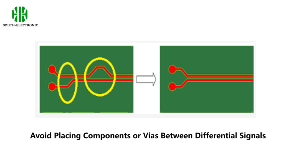
Tip 2: Avoid Placing Components or Vias Between Differential Signals
When you put stuff between the pairs, it screws up the impedance and causes reflections, which messes up the data. It screws up the impedance because it changes the impedance of the path, which screws up the differential pair’s ability to cancel noise and keep the signal clean. So, you want to keep the path of the pairs clear so the signals can go through without getting screwed up and keep working right.
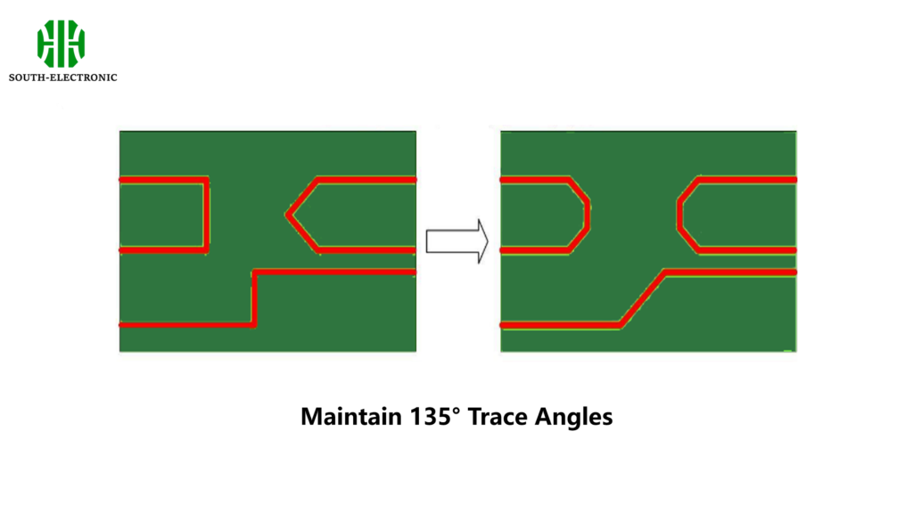
Tip 3: Maintain 135° Trace Angles
Sharp angles, especially 90° bends, can cause impedance discontinuities and signal reflections. This happens because sharp bends change the effective width of the trace, which leads to impedance variations. To avoid these issues, it is recommended to use 135° angles for trace bends. 135° angles provide a smoother transition for the signal, reducing the chances of signal degradation and improving overall performance.
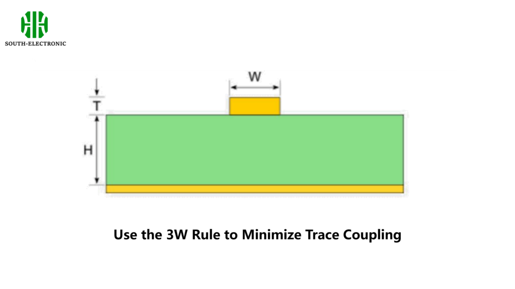
Tip 4: Use the 3W Rule to Minimize Trace Coupling
Crosstalk is a big problem in high-speed PCB designs. It‘s when signals in adjacent traces interfere with each other. To minimize crosstalk, you use the 3W rule. The 3W rule says that the spacing between traces should be at least three times the width of the traces themselves. By following the 3W rule, the electromagnetic fields generated by each trace are less likely to couple with adjacent traces, reducing the chances of crosstalk.
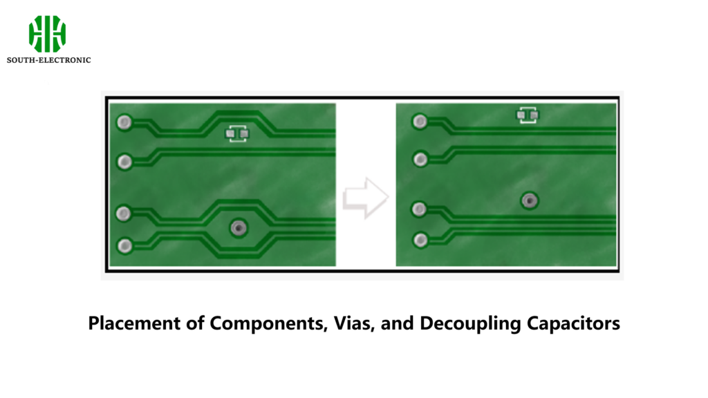
Tip 5: Placement of Components, Vias, and Decoupling Capacitors
Put your decoupling capacitors as close as you can to the power pins of your high-speed ICs. This way, you minimize the inductance of your power delivery network and give high-frequency noise a low-impedance path to follow. Also, if you place your vias right, you can reduce signal path lengths and avoid stubs that can cause signal reflections. Bottom line: carefully placing your components and vias will make your high-speed PCBs work better and last longer.
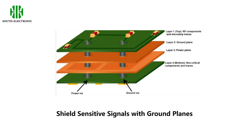
Tip 6: Shield Sensitive Signals with Ground Planes
Ground planes are important because they provide a stable reference plane for high-speed signals. They also help reduce EMI by absorbing and redirecting noise. By placing a continuous ground plane beneath high-speed signal layers, you can greatly reduce the potential for noise interference.
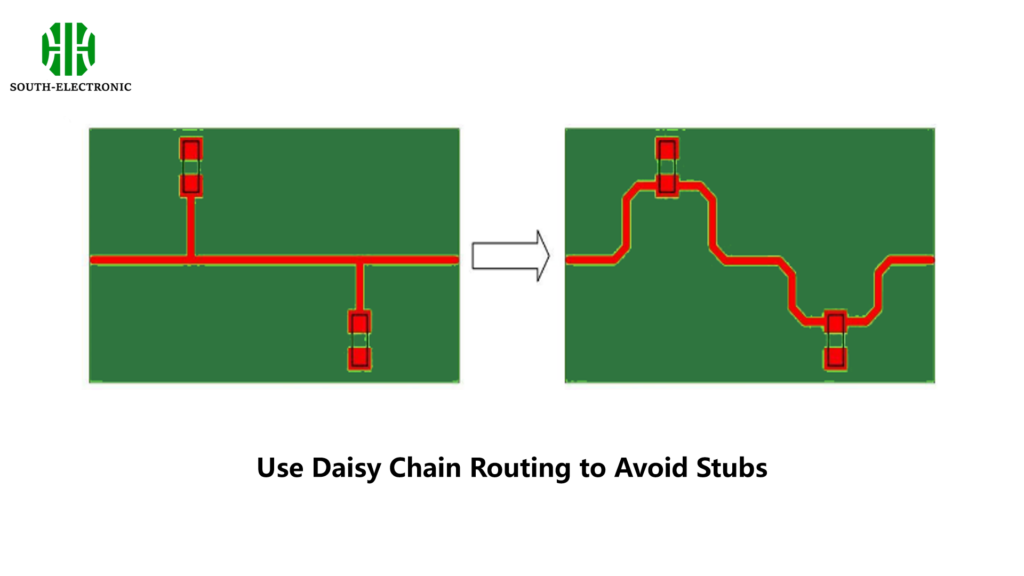
Tip 7: Use Daisy Chain Routing to Avoid Stubs
To avoid stubs, we use daisy chain routing. Daisy chain routing connects components in series, so the signal path is continuous and there are no branches. By using daisy chain routing, we maintain signal integrity and minimize the chance of signal reflections.
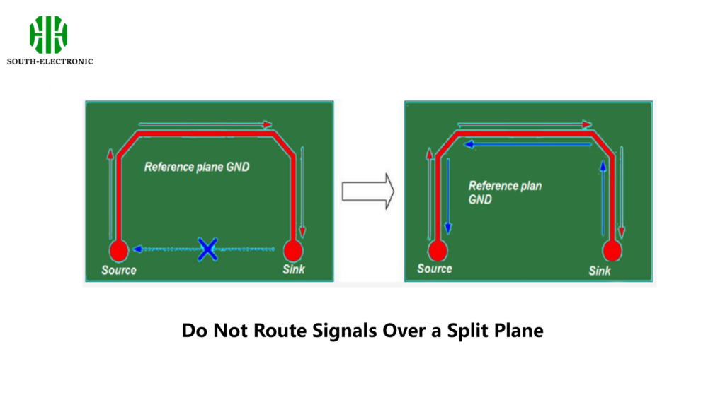
Tip 8: Do Not Route Signals Over a Split Plane
When you route high-speed signals over a split plane, you can cause impedance discontinuities and signal integrity problems. A split plane is when you have breaks or gaps in the reference plane. This can interrupt the signal path and cause reflections and noise. To maintain signal integrity, you need to make sure your high-speed signals have a continuous reference plane. This will prevent impedance mismatches and give the signal a solid ground, which will reduce noise and interference. You can avoid split planes and keep a consistent signal path by planning and laying out your board correctly.
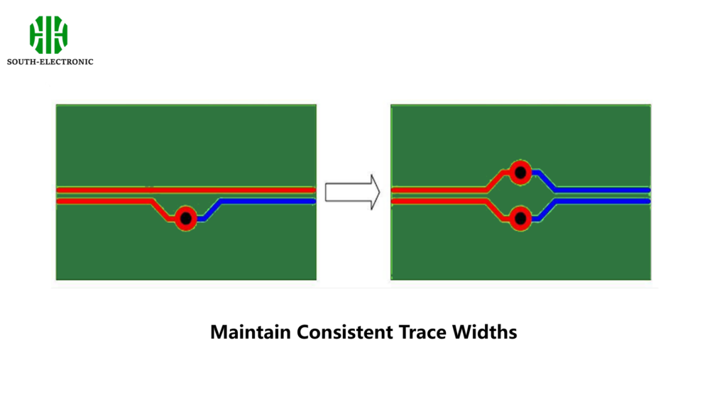
Tip 9: Maintain Consistent Trace Widths
If you don’t keep the width of your traces consistent, you’ll end up with impedance mismatches. That means your signals will bounce back and forth and get all messed up. To keep your traces the same width, you need to use good design tools and follow the manufacturer’s guidelines for trace dimensions. That way, the impedance stays the same all the way through your board, which means you won’t lose your signal and your high-speed stuff will work like it’s supposed to.
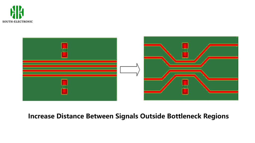
Tip 10: Increase Distance Between Signals Outside Bottleneck Regions
To reduce crosstalk, you need to increase the distance between high-speed signals, especially outside bottleneck regions. By increasing the spacing between signals, you reduce the potential for electromagnetic coupling, which minimizes the chances of crosstalk. This practice helps maintain signal integrity and reduce noise, which leads to better overall performance of the PCB.
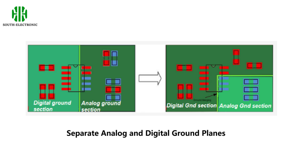
Tip 11: Separate Analog and Digital Ground Planes
By isolating analog and digital ground planes, the noise generated by digital circuits is contained and prevented from affecting the analog circuits. This practice enhances the performance and reliability of mixed-signal PCBs, ensuring that both analog and digital signals are transmitted accurately and without interference.
Conclusion
High-speed PCB routing is a complex but necessary part of modern electronics design. By following these 11 best practices, you can improve the performance and reliability of your high-speed circuits. Controlled impedance, minimizing signal paths, differential pair routing, and proper shielding are just a few of the important techniques that can help you achieve good signal integrity. Always validate your design through simulation to catch potential issues early and make sure your final product meets the necessary performance standards.

