
Due to the switching characteristics of switching power supplies, switching power supplies are prone to generate great electromagnetic compatibility interference. As a power engineer, electromagnetic compatibility engineer, or a PCB layout engineer, you must understand the causes and solutions of electromagnetic compatibility problems. In particular, layout engineers need to understand how to avoid the expansion of dirty spots. This article mainly introduces the key points of power PCB design.
29 basic relationships between layout and PCB
-
Several basic principles: Any wire has impedance; current always automatically chooses the path with the least impedance; radiation intensity is related to current, frequency, and loop area; common mode interference is related to the mutual capacitance of large dv/dt signals to ground; the principles of reducing EMI and enhancing anti-interference capabilities are similar.
-
The layout should be partitioned according to power supply, analog, high-speed digital and various functional blocks.
-
Try to reduce the area of large di/dt loops, reduce the length of large dv/dt signal lines (or area, the width should not be too wide, the increase in routing area increases the distributed capacitance, the general practice is: the routing width is as large as possible, but the excess part should be removed), and try to go straight to reduce its implicit surrounding area to reduce radiation.
-
Inductive crosstalk is mainly caused by large di/dt loops (loop antennas), and the induction strength is proportional to the mutual inductance, so it is critical to reduce the mutual inductance with these signals (the main way is to reduce the loop area and increase the distance); capacitive crosstalk is mainly generated by large dv/dt signals, and the induction strength is proportional to the mutual capacitance, so it is critical to reduce the mutual capacitance with these signals (the main way is to reduce the effective coupling area and increase the distance, and the mutual capacitance decreases faster with the increase of distance).
-
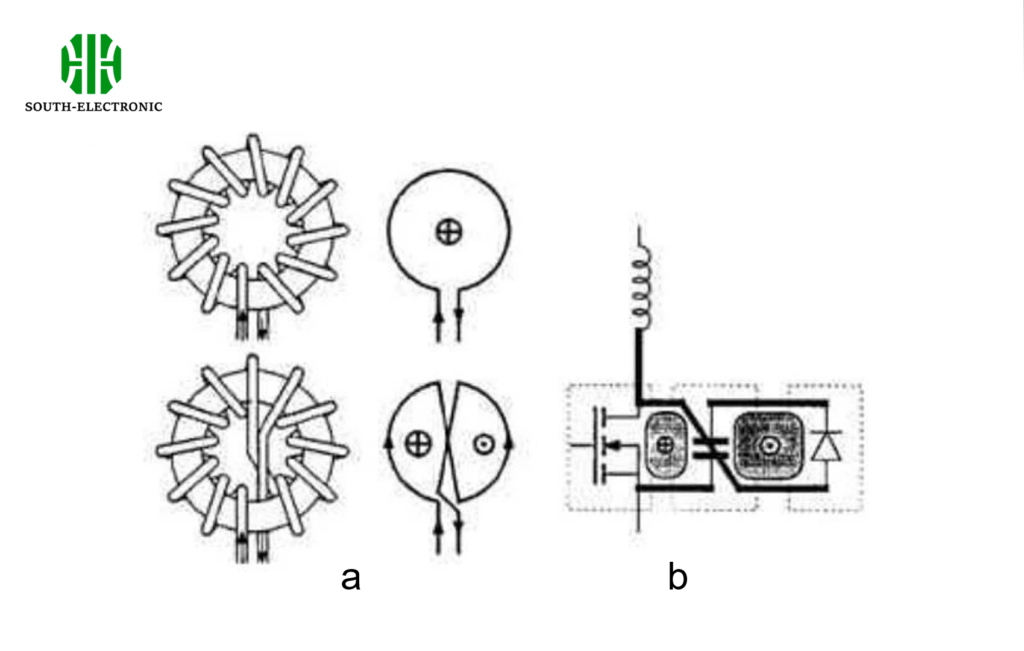
Try to use the principle of loop cancellation to route, and further reduce the area of the large di/dt loop, as shown in the figure below (similar to the twisted pair cable using the loop cancellation principle to improve anti-interference ability and increase transmission distance):
-
Reducing the loop area not only reduces radiation, but also reduces the loop inductance, making the circuit performance better.
-
Reducing the loop area requires us to accurately design the return path of each line.
-
When multiple PCBs are connected through connectors, it is also necessary to consider minimizing the loop area, especially for large di/dt signals, high-frequency signals or sensitive signals. It is best to have one signal line corresponding to one ground line, and the two lines are as close as possible. If necessary, they can be connected with twisted pair cables (the length of each turn of the twisted pair cable corresponds to an integer multiple of the half-wavelength of the noise). If you open the computer case, you can see that the motherboard to the front panel USB interface is connected with a twisted pair cable, which shows the importance of twisted pair cable connection for anti-interference and radiation reduction.
-
For data wiring, try to arrange more ground wires in the wiring, and make these ground wires evenly distributed in the wiring, so as to effectively reduce the loop area.
-
Although some inter-board connection lines are low-frequency signals, since these low-frequency signals contain a lot of high-frequency noise (through conduction and radiation), if they are not handled properly, it is also easy to radiate these noises.
-
When wiring, first consider high-current routing and routing that is prone to radiation.
-
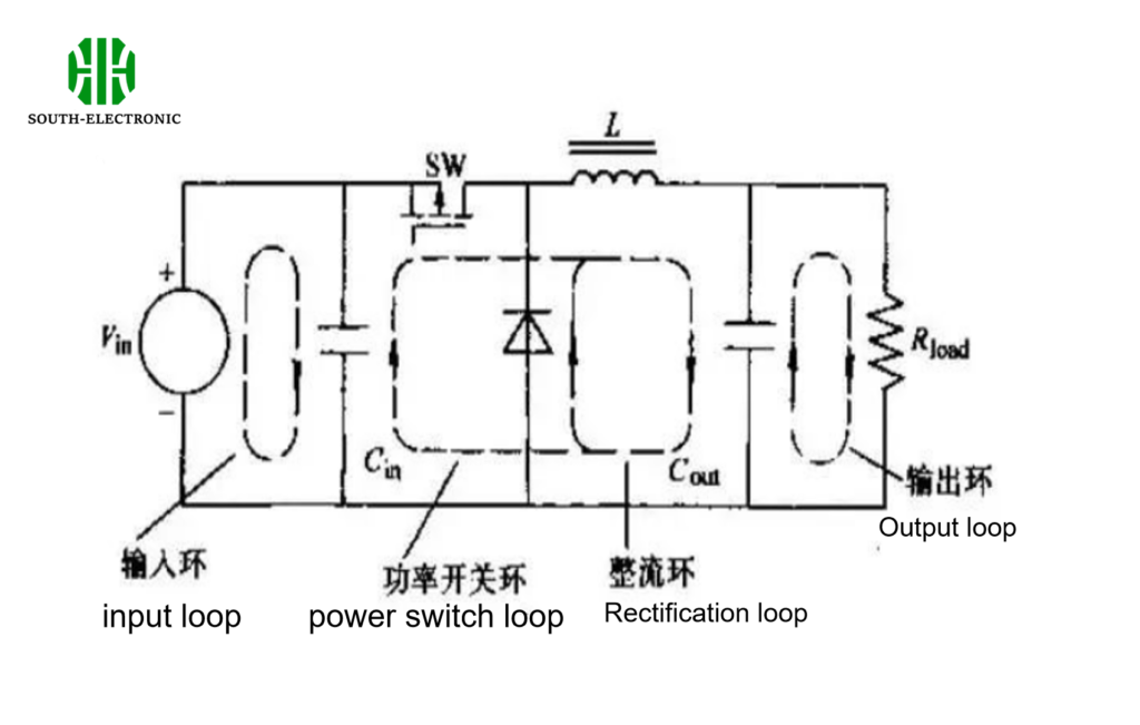
Switching power supplies usually have 4 current loops: input, output, switch, and freewheeling (as shown in Figure 2). Among them, the input and output current loops are almost DC, and almost no EMI is generated, but they are easily interfered; the switch and freewheeling current loops have large di/dt, which needs attention.
-
The gate drive circuit of MOS (IGBT) tubes usually also contains large di/dt.
-
Do not place small signal loops, such as control and analog circuits, inside large current, high-frequency and high-voltage loops to avoid interference.
-
Reduce the area and length of the signal loop that is susceptible to interference (sensitive) to reduce interference.
-
Keep small signal lines away from large dv/dt signal lines (such as the C pole or D pole of the switch tube, the snubber and the clamping network) to reduce coupling. You can lay a ground (or power supply, anyway, it is a constant potential signal) in the middle to further reduce coupling. The ground and the ground plane should be in good contact. Small signal lines should also be kept away from large di/dt signal lines as much as possible to prevent inductive crosstalk. It is best not to run small signal lines under large dv/dt signals. If the back of the small signal line can be laid with ground (same ground), it can also reduce the noise signal coupled to it.
-
A better approach is to lay ground around and on the back of these large dv/dt and di/dt signal traces (including the C/D poles of the switching device and the heat sink of the switching tube), connect the upper and lower layers of the ground with vias, and connect this ground to the common ground point (usually the E/S pole of the switching tube, or the sampling resistor) with a low-impedance trace. This can reduce radiated EMI. It should be noted that the small signal ground must not be connected to this shielded ground, otherwise it will introduce greater interference. Large dv/dt traces usually couple interference to the heat sink and nearby ground through mutual capacitance. It is best to connect the switch tube heat sink to the shielded ground. Using surface-mounted switching devices will also reduce mutual capacitance, thereby reducing coupling.
-
It is best not to use vias for traces that are prone to interference, as they will interfere with all layers passed through the vias.
-
Shielding can reduce radiated EMI, but due to the increased capacitance to the ground, the conducted EMI (common mode, or non-intrinsic differential mode) will increase. However, as long as the shielding layer is properly grounded, it will not increase much. It can be weighed in the actual design.
-
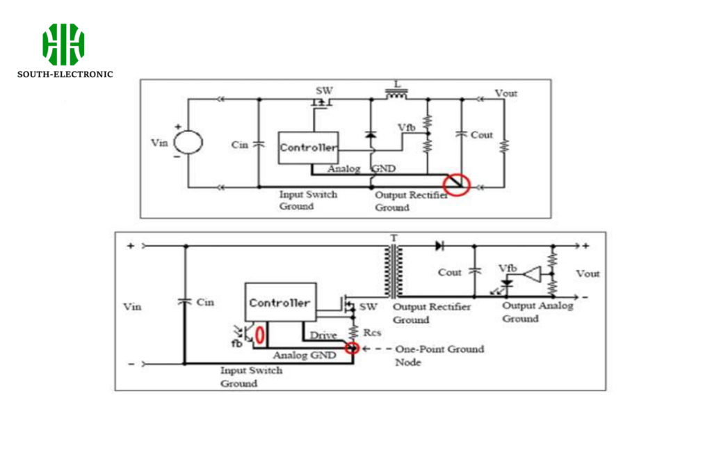
To prevent common impedance interference, use one-point grounding and lead the power from one point.
-
Switching power supplies usually have three types of ground: input power supply high current ground, output power supply high current ground, and small signal control ground. The ground connection method is shown in the following diagram:
-
When grounding, you should first determine the nature of the ground before connecting. The sampling and error amplification ground should usually be connected to the negative pole of the output capacitor, the sampling signal should usually be taken from the positive pole of the output capacitor, and the small signal control ground and drive ground should usually be connected to the E/S pole of the switch tube or the sampling resistor to prevent common impedance interference. Usually, the control ground and drive ground of the IC are not led out separately. At this time, the lead impedance from the sampling resistor to the above ground must be as small as possible to minimize common impedance interference and improve the accuracy of current sampling.
-
The output voltage sampling network is better to be close to the error amplifier rather than the output end. This is because low impedance signals are less susceptible to interference than high impedance signals. The sampling trace pairs should be as close to each other as possible to reduce the noise picked up.
-
Note that the inductors should be kept away from each other and perpendicular to each other in the layout to reduce mutual inductance, especially energy storage inductors and filter inductors.
-
Note that when high-frequency capacitors and low-frequency capacitors are used in parallel, the high-frequency capacitors should be close to the user.
-
Low-frequency interference is generally differential mode (below 1M), and high-frequency interference is generally common mode, usually through radiation coupling.
-
If the high-frequency signal is coupled to the input lead, it is easy to form EMI (common mode). A magnetic ring can be placed near the power supply of the input lead. If the EMI is reduced, it indicates that this problem exists. The solution to this problem is to reduce coupling or reduce the EMI of the circuit. If the high-frequency noise is not filtered out and is transmitted to the input lead, EMI (differential mode) will also be formed. In this case, the magnetic ring cannot solve the problem. Two high-frequency inductors (symmetrical) are connected in series near the power supply of the input lead. If the EMI is reduced, it indicates that this problem exists. The solution to this problem is to improve the filtering, or use buffering, clamping and other means to reduce the generation of high-frequency noise.
-
Measurement of differential mode and common mode current:
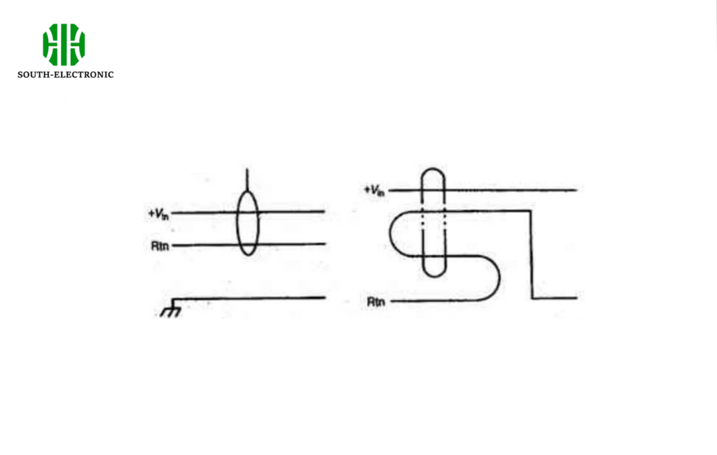
- The EMI filter should be as close to the incoming line as possible, and the incoming line should be as short as possible to minimize the coupling between the front and rear stages of the EMI filter. It is best to shield the incoming line with the chassis ground (the method is as described above). The output EMI filter should also be treated similarly. Try to keep the distance between the incoming line and the high dv/dt signal line as far as possible, and take this into consideration in the layout.

