

What is a Solder Mask Layer and Why is it Used?
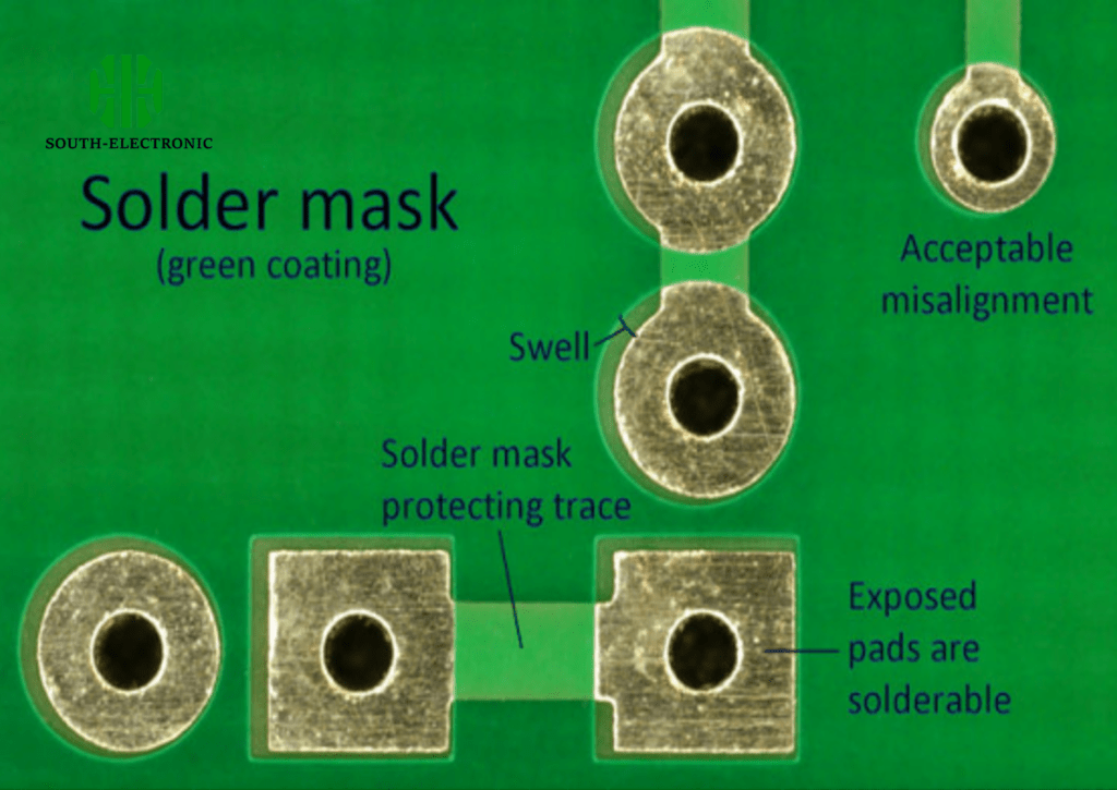
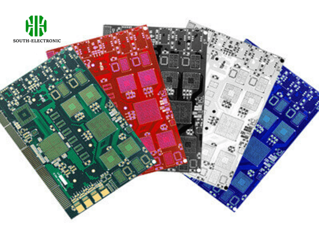
A solder mask layer, often called solder resist, is a thin polymer coating that’s put on the copper traces of a PCB. This layer insulates the conductive paths and protects them from environmental contaminants like moisture and dust. Solder masks are usually green, but they can also be red, blue, white, and other colors.
The Importance of Solder Mask Layers
Solder mask layers are essential in protecting circuit boards from various issues. Here are key benefits:
- Insulation During Soldering:The mask covers areas of the PCB where components are not soldered, ensuring components are placed correctly and preventing solder from bridging.
- Protection from Corrosion and Oxidation:Copper oxidizes when exposed to moisture and oxygen, losing its electrical properties. Solder resist prevents this by providing a protective layer.
- Prevention of Whisker Growth:Whiskers are thin metallic filaments that can cause short circuits. The solder mask helps prevent their formation.
- Reinforcement of Pads:The solder mask strengthens the copper pads, preventing them from separating from the PCB, which is crucial for maintaining structural integrity.
- Increased Breakdown Voltage:By applying the solder mask, the dielectric breakdown voltage of the PCB material is increased, enhancing its overall durability.
DFM Guidelines for Solder Mask Design
If you want to make sure your solder mask application is free of defects, you need to follow these four Design for Manufacturability (DFM) guidelines:
1. Employ Via Tenting
Tenting vias, where a via is covered with solder mask material, reduces exposed conductive pads and minimizes shorts during solder bridging. Liquid photoimageable (LPI) solder mask tenting is the most cost-effective method.
2. Minimum Solder Mask Web
The solder mask web should be at least 4 mils for green masks and 5 mils for other colors. This ensures adequate coverage and prevents unintended electrical connections.
| Solder Mask Web Width | Color |
|---|---|
| 4 mil | Green |
| 5 mil | Others |
3. Maintain a 1:1 Ratio for Solder Mask Openings
The solder mask openings should match the underlying copper pads to avoid unnecessary exposure and potential damage.
4. Accurate Pad Sizes for SMD and NSMD Pads
Solder mask-defined (SMD) pads have the mask opening smaller than the pad, while non-solder mask-defined (NSMD) pads have a gap between the pad and the mask. Accurate alignment is essential for optimal soldering.
Types of Solder Masks
Various types of solder masks are used depending on the application:
- Top and Bottom Masks:These identify openings in the green solder resist and are added through epoxy or film methods.
- Epoxy Liquid Solder Masks:The most cost-effective option, applied via silkscreening followed by thermal curing.
- Liquid Photoimageable (LPI) Solder Masks:A mix of liquids applied through curtain coating, screen printing, or spray applications. They offer a thin, durable coating.
- Dry Film Photoimageable Solder Masks:Require vacuum lamination and are ideal for high-density wiring boards due to their precise application.
Standard Thickness and Colors
The standard thickness of a solder mask layer is at least 0.8 mil, with some areas potentially being as thin as 0.3 mil. The color of the solder mask does not affect electrical properties but does affect visibility, inspection, and aesthetics.
| Solder Mask Color | Features |
|---|---|
| Green | Most common, highest resolution due to superior UV light absorption |
| Red/Blue | Similar resolution to green |
| Black | Lowest contrast, making visibility and inspection difficult |
| White | Rarely used due to poor visibility, ideal for LED applications |
| Transparent | Provides superior detail and resolution |
Key Takeaways
- Solder masks are critical for protecting PCBs from environmental damage and ensuring optimal functionality.
- DFM guidelines help avoid defects in solder mask application, ensuring a reliable end product.
- Different types of solder masks are available to suit various applications, with green being the most common color.
- Proper thickness and color selection are important for the performance and inspection of PCBs.
By understanding and implementing these guidelines, you can ensure the reliability and longevity of your PCBs, ultimately leading to better product performance and customer satisfaction.


