
What is Laser Direct Imaging (LDI)?
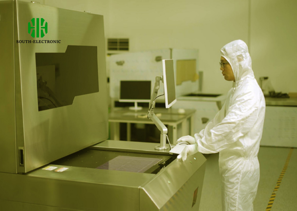
Laser Direct Imaging is an advanced photolithographic process that eliminates the need for physical phototools. Laser Direct Imaging (LDI) has revolutionized the printed circuit board (PCB) manufacturing industry. By directly exposing digitally saved patterns onto the photoresist without the need for a phototool, LDI offers unmatched precision, speed, and environmental benefits.
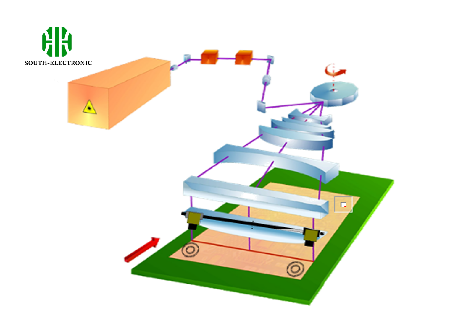
The LDI Process
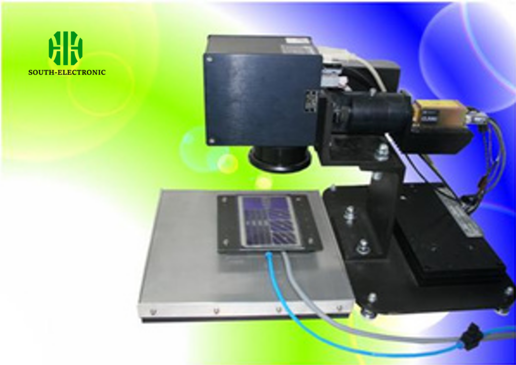
Laser Direct Imaging is an advanced photolithographic process that eliminates the need for physical phototools. Instead, it uses a computer-controlled laser beam to transfer the circuit design directly onto the photoresist layer of the PCB. The process involves several key steps:
- Preparation: The PCB substrate is cleaned and prepped, ensuring no contaminants affect the imaging process.
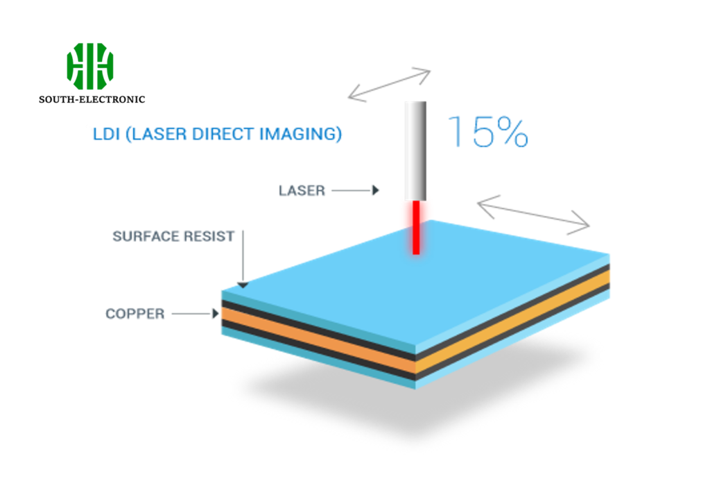
- Coating with Photoresist: A photosensitive layer is applied to the substrate, which will be exposed by the laser.
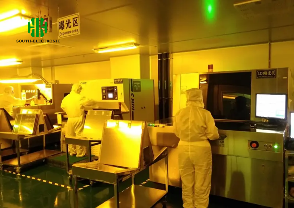
- Laser Exposure: The laser precisely exposes the design onto the photoresist, rastering across the surface in a controlled manner.
- Development and Etching: The exposed areas of the photoresist are developed, and unexposed areas are etched away, revealing the desired circuit pattern.
- Post-Processing: The board is cleaned and inspected for quality assurance.、
Comparing LDI with Traditional Photolithography
Traditional photolithography relies on phototools—masks created from drawings—that are used to project circuit patterns onto the PCB. This method, while effective, has several drawbacks:
- Inflexibility: Phototools are static, making design changes cumbersome and costly.
- Environmental Sensitivity: Phototools can degrade due to dirt, scratches, and environmental factors like temperature and humidity.
- Lower Precision: Light diffraction and alignment issues can lead to less precise circuit patterns.
LDI, in contrast, offers flexibility and precision, with the ability to adapt designs digitally and eliminate issues related to phototool degradation.
Quality Comparison Between LDI and Traditional Photolithography
| Aspect | LDI | Traditional Photolithography |
|---|---|---|
| Line Precision | Up to 5 microns | 10-15 microns |
| Image Quality | Consistent and sharp | Variable, affected by phototool quality |
| Design Flexibility | High, due to digital design files | Low, requires new phototools |
| Environmental Sensitivity | Low | High |
Advantages of Laser Direct Imaging (LDI)
Enhanced Quality and Precision
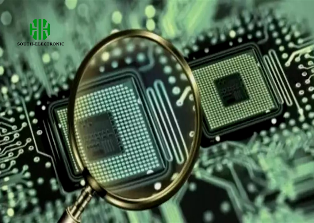
One of the most significant advantages of LDI is its ability to produce high-quality, precise circuit patterns. The laser’s direct exposure method allows for finer lines and more detailed designs, which are crucial for high-density interconnect (HDI) boards.
Speed and Efficiency
LDI streamlines the PCB manufacturing process by eliminating the need for phototool creation and setup. This reduction in steps not only speeds up production but also reduces potential points of failure.
- Faster Prototyping: LDI allows for rapid iteration of designs, which is especially beneficial during the prototyping phase.
- Higher Throughput: With fewer steps and less downtime, LDI can produce more boards in a shorter time frame.
Cost-Effectiveness
While the initial investment in LDI technology may be higher, the long-term cost savings are substantial. The elimination of phototool production, reduced waste, and faster production times all contribute to a lower total cost of ownership.
| Cost Aspect | Initial Cost | Long-Term Cost (5 years) | Notes |
|---|---|---|---|
| Phototool Creation | None | N/A | Not required in LDI |
| Equipment Maintenance | Medium | Low | Fewer parts to maintain |
| Material Costs | Low | Lower | Less chemical use and material waste |
| Overall Cost | Higher | Lower | Initial investment offset by operational savings |
Case Studies and Applications
LDI has proven invaluable in various industries, from consumer electronics to aerospace. For example, in the production of smartphones, where space is at a premium and precision is paramount, LDI’s ability to create fine lines and spaces ensures optimal component placement and performance. In aerospace, LDI’s precision and reliability make it ideal for crafting complex circuit boards required for navigation and communication systems.
Future Trends in LDI Technology
The future of LDI looks promising, with ongoing developments aimed at further enhancing its capabilities. These include:
- Integration with 3D Printing: Combining LDI with additive manufacturing techniques for more complex and integrated circuit designs.
- Automation and AI Integration: Using AI to optimize the imaging process, improving accuracy and efficiency.
- Material Innovations: Developing new photoresist materials that are even more responsive to laser imaging, enabling finer detail and faster processing.
As technology evolves, LDI is set to become even more integral to PCB manufacturing, pushing the boundaries of what is possible in electronics design.
Laser Direct Imaging (LDI) offers a range of benefits over traditional photolithography, including higher precision, faster processing times, reduced environmental impact, and greater cost-effectiveness. As industries continue to demand more complex and reliable PCB designs, the adoption of LDI is likely to grow, cementing its place as a cornerstone technology in electronics manufacturing.

