

Have you ever wondered how your USB device transfers data at lightning speed? Behind every flash drive lies an unsung hero: the USB PCB. Let’s uncover the engineering marvel powering your daily tech interactions.
A USB PCB[^1] is a printed circuit board specifically designed for USB applications. It uses copper traces to manage data/power transfer between connectors, with precise impedance control and EMI shielding[^2] to meet evolving USB standards from 2.0 to USB4.
While basic in concept, USB PCBs hide surprising complexity. Their performance determines whether your file transfer succeeds in seconds or frustrates for minutes. Let’s dismantle one layer by layer.
Introduction to USB PCB
Your smartphone’s charging hiccup might trace back to a poorly designed USB PCB. These boards form the nervous system of USB devices, routing signals through microscopic pathways thinner than human hair.
USB PCBs are multilayer boards[^3] (4-8 layers typically) containing critical pathways for power delivery (VBUS), data transfer (D+/D-), and ground connections. Their stackup varies by USB generation, with USB4 requiring advanced materials for 20Gbps+ speeds.
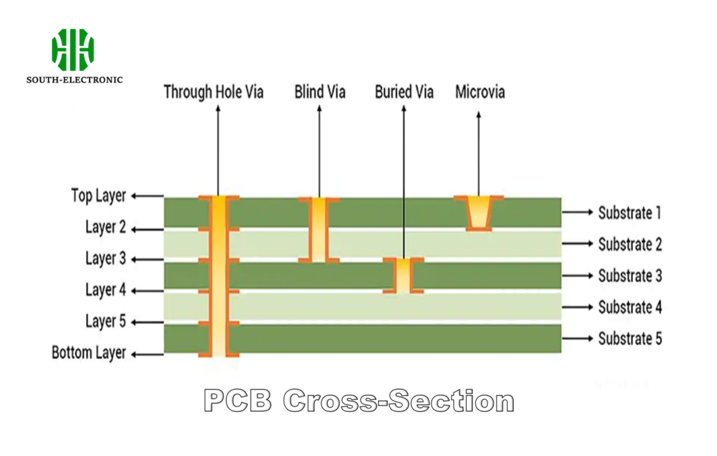)
Anatomy of Modern USB PCBs
| Layer Type | Purpose | Material Choices | Thickness Range |
|---|---|---|---|
| Signal | Data transfer | High-frequency laminates (Rogers 4350B) | 0.1-0.3mm |
| Power | Voltage distribution | Standard FR-4 with thick copper | 0.2-0.5mm |
| Ground | EMI control | Copper-filled via arrays | Full layer |
| Dielectric | Insulation | Polyimide or PTFE | 0.05-0.2mm |
Contemporary USB designs battle against signal attenuation – a 3-inch USB 3.2 Gen 2×2 cable loses up to 15% signal strength without proper impedance matching. Advanced designs use corner stitching techniques where 90° trace angles get replaced by two 45° bends, reducing reflections by 37% (IPC-2141A standard). Differential pair routing maintains precise 100Ω impedance through calculated trace width/spacing ratios.
Key Components of a USB PCB
Why do some USB-C cables cost $5 while others hit $50? The answer lives in their PCB components. Every millimeter matters when handling 100W power and 40Gbps data.
Essential components include Type-A/B/C connectors, TVS diodes for surge protection, impedance-controlled differential pairs[^4], and dedicated E-Marker chips for USB PD compliance[^5]. Component placement follows strict USB-IF layout guidelines.
)
The $0.03 Component That Makes or Breaks USB
| Component | Function | Cost Range | Failure Impact |
|---|---|---|---|
| EMI filter | Reduces noise | $0.03-$0.15 | Data errors |
| CC resistor | Connection detection | $0.01 | Charging failure |
| Ferrite bead | High-frequency suppression | $0.02 | Signal degradation |
| Via fence | EMI containment | $0.05 (per 100 vias) | Cross-talk |
The humble CC (Configuration Channel) resistor dictates cable functionality. A 5.1kΩ resistor (±1% tolerance) enables basic USB-C charging, while advanced setups use Ra/Rd resistors in precise configurations. Poor resistor selection caused early USB-C cables to fry devices – a $0.01 component risking $1000 phones. Modern designs integrate multilayer ceramic capacitors (MLCCs) with X7R dielectric for stable performance across -55°C to +125°C.
Why Material Choice Matters in USB PCB Manufacturing?
Your USB cable’s performance plummets in winter? Material selection explains this thermal sensitivity. Substrate materials dramatically affect signal integrity across temperature ranges.
FR-4 works for USB2.0, but USB3.2+ demands low-Dk materials[^6] like Isola 370HR or Taconic TLY-5. These maintain stable dielectric constants (Dk ±0.05) across -50°C to +150°C, critical for 10Gbps+ transfers.
)
Material Showdown: Cost vs Performance
| Material | Dk @ 1GHz | Df | Cost/cm² | Max Frequency |
|---|---|---|---|---|
| FR-4 | 4.5 | 0.02 | $0.15 | 3GHz (USB3.2) |
| Rogers 4350B | 3.48 | 0.0037 | $2.10 | 30GHz (USB4) |
| Megtron 6 | 3.7 | 0.002 | $1.80 | 25GHz |
| PTFE | 2.1 | 0.0004 | $3.50 | 50GHz |
FR-4’s dielectric loss (Df=0.02) becomes problematic beyond 5Gbps – a USB4 signal would lose 40% power in 6-inch traces. High-speed materials use filler-controlled glass weave to prevent "weave effect" distortion. For cost-sensitive designs, hybrid stackups combine FR-4 cores with high-speed prepreg, cutting material costs by 60% while maintaining 85% performance. Thermal management remains critical; some USB PD boards integrate 2oz copper layers for 100W power delivery without overheating.
Designing a USB PCB: Key Challenges and Solutions
Ever fried a USB port? Poor PCB design often bears the blame. The shift to USB4 brings 80Gbps speeds, requiring millimeter-perfect engineering.
Key challenges include maintaining 85Ω differential impedance[^7], suppressing SSO noise below 50mVpp, and achieving insertion loss < -3dB at Nyquist frequency. Solutions involve corner chamfering, via stitching, and adaptive equalization circuits.
Battle Plan for USB4 Compliance
| Challenge | Parameter | Solution | Tolerance |
|---|---|---|---|
| Impedance mismatch | ±10% allowed | TDR tuning | ±7% target |
| Crosstalk | <5% | Ground guard traces | -30dB isolation |
| Power integrity | 20mV ripple | Bulk + MLCC capacitors | 10mV achieved |
| EMI | FCC Class B | Via fencing + shielding | 3dB margin |
Differential pair routing demands mathematical precision. For USB4's 80Gbps (PAM3 encoding), trace length matching must stay under 2mil (0.05mm) – thinner than paper. Advanced HDI boards use laser-drilled microvias (0.1mm diameter) to connect layers without stub effects. Simulation tools like Ansys SIwave model insertion loss down to 0.1dB accuracy, predicting eye diagrams before fabrication. Some designers embed resistors into PCB substrates (RDL technology) to save space and reduce parasitic inductance by 40%.
Conclusion
USB PCBs are technological chameleons – simple in concept yet demanding nanoscale precision. From material science to signal integrity, their design defines our connected world's reliability and speed. Modern USB-C alone contains more engineering than the Apollo guidance computer.
[^1]: Explore this link to understand the intricate design and functionality of USB PCBs, essential for modern data transfer.
[^2]: Learn about EMI shielding’s role in preventing interference, ensuring reliable performance in USB devices and beyond.
[^3]: Discover the benefits of multilayer boards in electronics, crucial for efficient data and power management in devices.
[^4]: Learn about impedance-controlled differential pairs to enhance your knowledge of USB signal integrity and design.
[^5]: Discover the role of E-Marker chips in USB PD compliance to ensure safe and efficient power delivery.
[^6]: Explore this link to understand how low-Dk materials enhance signal integrity in high-speed USB applications.
[^7]: This resource will provide insights into techniques for achieving optimal differential impedance in USB PCB designs.

