
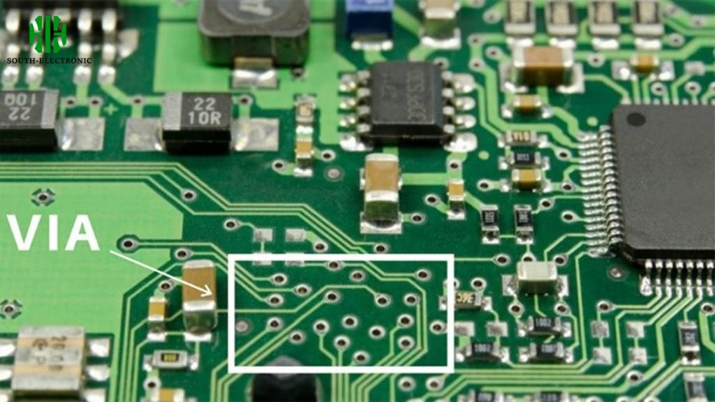
What Are Vias in PCB Design?
A via is used to connect copper layers on a PCB, while a PTH is generally larger than a via and is used as a plated hole to accept component leads, such as non-SMT resistors, capacitors, and DIP package ICs. They are small holes drilled into the PCB that are plated with a conductive material, usually copper. These holes allow signals and power to be routed vertically through the PCB stack-up, connecting various layers as needed by the circuit design.
Typical Vias design rules
| Design Rule | Description |
|---|---|
| Minimum Via Diameter | Smallest allowed diameter for via holes |
| Minimum Annular Ring | Required ring of copper around via holes |
| Via Aspect Ratio | Ratio of via depth to its diameter |
| Backdrilling Requirements | Conditions under which backdrilling is used |
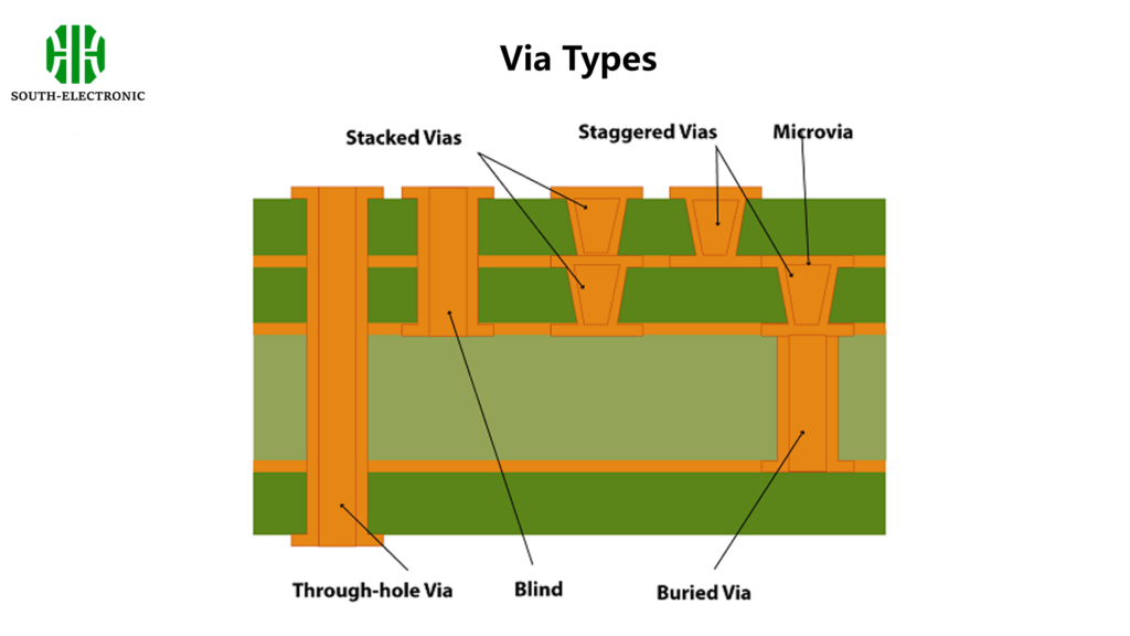
What are the Different Types of Via Commonly uUsed in PCBs?
- Through vias: Through-hole vias are drilled from the top to the bottom of the PCB, connecting all layers in between. They are the most straightforward type of via and are commonly used in simpler PCB designs.
- Blind vias: Blind vias connect an outer layer to one or more inner layers but do not extend through the entire board. They are used in high-density interconnect (HDI) designs to save space.
- Buried vias: Buried vias connect two or more inner layers without reaching the outer layers. They are completely encapsulated within the PCB and are also used in HDI designs.
- Microvias: These are very small vias with a diameter typically less than 0.006 inches. They usually connect just one layer to an adjacent layer and are often used in high-density interconnect (HDI) PCBs.
How do Choose the Right Type of Vias for a Particular Application?
Key considerations for selecting via types:
| Via Type | Signal Integrity | Thermal Management | Manufacturing Cost | Typical Applications |
|---|---|---|---|---|
| Through-Hole | Moderate | Moderate | Low | General-purpose, low-complexity designs |
| Blind | High | High | Moderate | High Density Interconnect (HDI), space-constrained designs |
| Buried | High | High | High | High Density Interconnect (HDI), high-density interconnects |
| Microvias | Very High | Moderate | High | High-performance, multi-layer, compact devices, smartphones, advanced wearable technology |
What role do Vias play in multilayer PCBs?
In multilayer PCBs, vias play a critical role in achieving the desired circuit functionality and performance by providing:
- Interlayer connectivity: Vias are the primary means of connecting circuits on different layers, which is essential in multilayer PCBs where space is limited and circuit complexity is high.
- Signal routing flexibility:Vias let you route signals between different layers, which helps you avoid noise and optimize your layout for signal integrity.
- Thermal management: Especially in high-power applications, vias can help dissipate heat by connecting heat-generating components to heat sinks or other thermal management layers.
Vias are indispensable in multilayer PCB design, enabling the vertical integration of circuits that, in turn, allows for the miniaturization and functional enhancement of electronic devices.

