
Wearable PCB Suppliers
South-Electronic
At South-Electronic, we are committed to providing quality wearable PCB that enhance connectivity, reliability, and functionality, ensuring your devices operate seamlessly and intelligently.
Get the Best Wearable PCB with us and Enjoy Unmatched Quality
Welcome to South-Electronic, your trusted source for wearable PCB, our PCB is built to power your applications, from cutting-edge fitness trackers to advanced healthcare monitoring devices.
Trust South-Electronic for exceptional quality and reliability in your wearable technology projects.
Partner with us to bring innovation and user satisfaction to your industry.
Fitness & Wellness PCB
Made for devices that track your health, monitor your activity, and help you stay well. These are the circuit boards that go into wearables like fitness bands, smartwatches, and health monitors. They have stuff like biometric sensors and wireless chips built in.

Medical & Healthcare PCB
Specialized PCB for medical-grade wearables. These include devices for patient monitoring, chronic condition management, and emergency medical response. Emphasizing high reliability and compliance with medical standards.
Consumer Electronics PCB
Made for consumer wearables like smartwatches, smart glasses, and other connected accessories. The PCB is for a broad consumer audience, and they focus on connectivity, compactness, and energy efficiency.
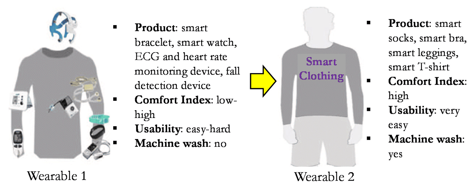
Smart Clothing & Textiles PCB
ThePCB are designed to be integrated into smart textiles and smart clothing, providing seamless connectivity and new functions in everyday clothing. They are perfect for fashion and functional wearables, and can be used to create heated clothing, illuminated garments, or garments that respond to the wearer.
Why Choose South-Electronic?
- High-Quality Manufacturing
Your devices require the best, and we deliver.
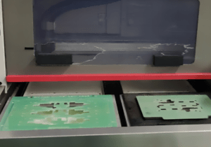
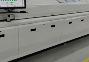
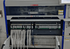
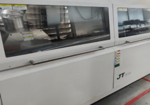
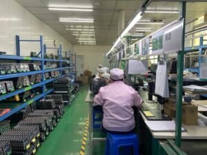
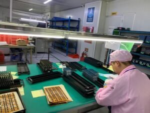
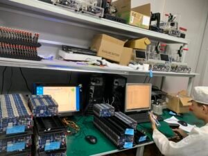
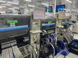
With 8 advanced production lines, our factory ensures that every PCB we manufacture meets the highest standards of quality and reliability. - Advanced Technology Integration
Your ideas are backed by state-of-the-art technology.
We're on the integrating the latest in connectivity and miniaturization. Our boards are designed to support all the key communication protocols for wearable tech, including Bluetooth, NFC, and Wi-Fi. - Speed to Market
Your timeline matters, and we respect that.
We shorted the design-to-production process so we can complete your project faster. We can quickly help you go from prototyping to full production, allowing you to stay competitive in the fast-paced wearable market. - Eco-Friendly Production
Your commitment to sustainability is shared by us
We use environmentally friendly materials and manufacturing processes, so we can help you reduce your ecological footprint. This is good for the planet, and it also resonates with consumers who value environmentally conscious. - Global Reach with Local Support
Your global presence is supported locally.
South-Electronic is headquartered in China with a strong export presence in Europe and the U.S. We provide local customer support in these regions, ensuring smooth communication and rapid responses.
Related Project We had Done
Customer Reviews
Common Questions
Most Popular Questions
Send us a message
The more detailed you fill out, the faster we can move to the next step.


The Complete Guide For Wearable PCB
Content
Chapter 1

Introduction to Wearable PCB
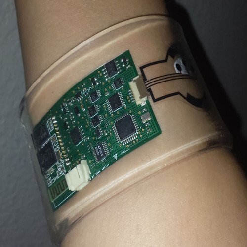
Overview of Wearable PCB Technology Wearable PCB is the foundation of the rapidly growing field of wearable technology. The specialized PCB is small, flexible, and rugged, making them easy to install into a variety of wearable devices. Unlike traditional PCB, wearable PCB must be able to withstand stresses such as bending and twisting, and often require special materials and manufacturing processes to meet these requirements. They integrate key components such as microcontrollers, sensors, and connectivity modules to enable advanced features such as health monitoring and enhanced connectivity.
Importance in Modern Electronics How important are wearable PCB in modern electronics? Wearable PCB is key to driving innovation in modern electronics, revolutionizing the way we interact with technology on a daily basis. They are essential to the functionality and usefulness of devices such as smart watches, fitness trackers, and medical monitoring devices. Not only do these PCB make devices more user-friendly and easy to use, but they are also able to collect and transmit data in real time, making wearable technology more useful in our daily lives. Their development is in line with the growing trend of the Internet of Things (IoT), where connectivity and data exchange are crucial.
Evolution of Wearable PCBs in the Tech Landscape The development of wearable PCB reflects the broader trend of technology toward miniaturization, personalized medicine, and ubiquitous computing. From early simple wearable device applications, PCB have evolved to accommodate more complex applications, incorporating organic materials and advanced polymers to provide greater flexibility and biocompatibility. Technological advances have also led to more energy-efficient designs and the integration of nanoscale components, pushing the limits of what can be achieved in wearable devices. This development is not only about technological improvements, but also about how these devices are increasingly integrated into daily life, addressing everything from fitness and fashion to chronic disease management and elderly care.
By understanding these basic aspects, one can appreciate not only the technical complexity involved in designing and manufacturing wearable PCBs but also their critical role in shaping the future of personal electronics.
Chapter 2
Design Principles for Wearable PCB
Key Design Considerations When designing a PCB for a wearable device, there are several important factors to consider to ensure that the end product works properly, is reliable, and is easy to use. The main things to consider include:
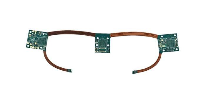
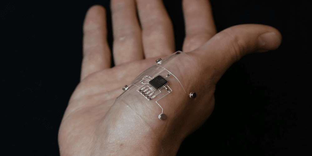
Flexibility: Wearable devices often need PCB that can bend and twist without breaking. Flexible PCB, made with materials that can withstand mechanical stress, are essential in such applications.
Compactness: Wearable devices have limited space, so PCB must be designed to be as small as possible while still hosting all necessary components. This means meticulous layout planning and multi-layer configurations to maximize space without sacrificing performance.
Power Consumption: Wearable devices usually run on small batteries with limited capacity, so low power consumption is a key design consideration. Designers must optimize the PCB for energy efficiency, choosing low-power components and using power management techniques to maximize battery life.
Material Selection for Wearability and Durability The materials used in wearable PCB affect not only their performance but also their comfort and durability. When selecting materials, designers must consider:
Biocompatibility: Materials that touch your skin should be non-toxic and hypoallergenic so they don’t irritate you or cause a rash.
Flexibility and Strength: Materials like polyimide are often used for flexible PCB because they offer excellent mechanical properties and can withstand environmental stressors like moisture and heat.
Durability: Wearable devices get exposed to all sorts of things, like sweat, dust, and mechanical stress. You need materials that can handle that without falling apart.
Case Studies of Successful Wearable PCB Designs Here are a few examples of successful wearable PCB designs that demonstrate these principles in action:
Fitness Trackers: A leading fitness tracker brand uses a multi-layer, flexible PCB that’s lightweight and durable. The device incorporates ultra-low-power components to monitor heart rate and activity while maintaining battery life for up to a week on a single charge.
Smartwatches: Another example is a popular smartwatch that uses a small, rigid-flex PCB to keep the profile slim and include multiple sensors and connectivity options. This design supports features like GPS, Wi-Fi, and cellular connectivity without killing the battery.
Medical Monitoring Devices: We’re working on a really cool project where we’re developing a wearable ECG monitor. We’re using a flexible PCB that’s coated with a biocompatible material. This device can continuously monitor your heart rate and other vital signs. It’ll give doctors and nurses the information they need to take care of you, and it’s comfortable to wear.
These case studies show how important it is to think about how you design your wearable PCB products and what materials you use. If you follow these principles, you can make devices that are not only really cool and high-tech, but also practical and tough enough to use every day.
Chapter 3
Types of Wearable PCB
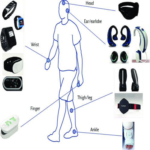
Classification Based on Application Wearable PCB can be classified into several categories based on their specific applications. These include:
Fitness: PCB designed for fitness wearables, such as activity trackers and smart sportswear, focus on durability and the ability to integrate sensors that monitor physical activities like steps, heart rate, and calorie consumption.
Medical: The PCB is used in medical devices worn by patients to monitor health conditions continuously. Examples include wearable ECG monitors, blood pressure cuffs, and glucose monitors. The design emphasizes accuracy, reliability, and compliance with medical standards.
Consumer Electronics: This broad category includes PCB for devices like smartwatches, smart glasses, and other wearable tech that enhances everyday life. The PCB often incorporate a variety of functionalities including communications, enhanced media capabilities, and integration with other smart devices.
Differences Between Each Type and Their Specific Requirements
Fitness PCB require robustness to withstand physical activities and environmental factors such as sweat, dirt, and varying temperatures. They must also be highly flexible and lightweight to ensure comfort during prolonged wear.
Medical PCB is subject to stringent regulatory standards. They must ensure high precision and stability to provide reliable health data. Biocompatibility is also crucial, as these devices often come into direct contact with the wearer’s skin or even with their bloodstream in some cases.
Consumer Electronics PCB needs to support a wide range of functionalities and therefore often require high-density interconnect (HDI) PCB. The PCB must also support multiple communication protocols like Bluetooth, NFC, and Wi-Fi, and they need to be aesthetically pleasing since they are often visible on the user.
Innovations in Each Category
Fitness: Innovations in fitness PCB include the integration of advanced sensors that can track not only physical activity but also physiological parameters like skin temperature and galvanic skin response. Energy-harvesting technologies are also being explored to extend battery life.
Medical: Recent advances in medical wearable PCB include the development of more compact and flexible designs that can provide continuous, real-time health monitoring without impacting the wearer’s daily activities. Additionally, there’s a growing focus on incorporating AI algorithms directly into the PCB to provide instant health insights and alerts.
Consumer Electronics: In the consumer sector, innovations focus on enhancing the interactivity and connectivity of wearable devices. This includes the integration of haptic feedback, more sophisticated and energy-efficient displays, and seamless integration with other smart devices in the IoT ecosystem.
These categories and innovations highlight the diverse applications of wearable PCB and the specialized requirements needed to meet the expectations of different users and use cases. As technology advances, the distinctions between these categories may blur, leading to more integrated and multifunctional wearable devices.
Chapter 4
Key Components of Wearable PCB
Key Components
Microcontrollers: The microcontroller is like the brain of the wearable. It takes in data from the sensors, does some thinking, and then makes things happen. It runs the software that controls what the device does and how you interact with it.
Sensors: Sensor is super important for gathering data about the person wearing the device or the environment around them. Common sensors in wearables include accelerometers, gyroscopes, heart rate monitors, and temperature sensors. These sensors let the device track your fitness activity, keep an eye on your health metrics, or even tell you when something in the environment changes.
Power Supplies: Most wearable devices are powered by batteries, particularly rechargeable lithium-ion or lithium-polymer batteries, due to their compact size and efficiency. Power management circuits are also essential to ensure battery longevity, especially in devices intended for continuous wear.
Selection Criteria for Components Based on Device Requirements
Compatibility: Components must be compatible with each other and with the overall system architecture to ensure smooth integration and operation.
Power Efficiency: Components should be chosen based on their power consumption profiles. Low-power components are preferred to extend the battery life of the device, which is crucial for user satisfaction.
Size and Flexibility: For wearables, components need to be compact and, in some cases, flexible. This is particularly important for devices that are worn on softer parts of the body, like wristbands or clothing.
Durability and Reliability: Given that wearables are exposed to various physical activities and environmental conditions, components must be robust and reliable.
Integration Techniques for Maximizing Efficiency and Functionality
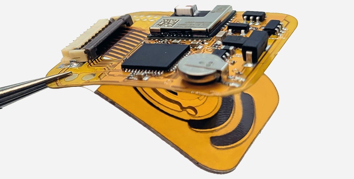
Multi-layer PCBs: Utilizing multi-layer PCBs can help in accommodating more circuitry within a limited space, which is crucial for the compact design of wearable devices.
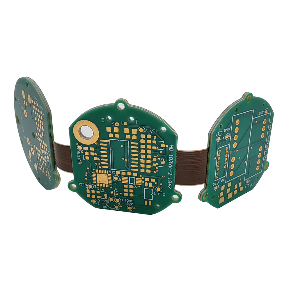
Rigid-Flex PCB: Combining rigid and flexible PCB technologies allows for the creation of complex electronic devices that are both space-efficient and durable. Rigid-flex PCB is particularly useful in wearables due to their ability to bend during use while providing a stable platform for mounting components.
Modular Design: Designing the PCB with modular sections can simplify both the assembly process and any necessary repairs or upgrades. This approach also allows for easier customization of the device for different markets or user preferences.
Energy Harvesting Techniques: Integrating energy-harvesting components, such as solar cells or thermoelectric generators, can help supplement battery power and extend the device’s usage time between charges.
Advanced Packaging Techniques: Employing advanced component packaging techniques such as system-in-package (SiP) or chip-scale package (CSP) can reduce the overall footprint of the components on the PCB, freeing up space for additional functionalities.
By carefully selecting components and employing innovative integration techniques, designers can create wearable PCB that are efficient, functional, and tailored to meet the specific needs of different applications. This results in wearable devices that are not only technologically advanced but also user-friendly and durable.
Chapter 5
Connectivity Solutions for Wearable Devices
Overview of Connectivity Options
Bluetooth: Bluetooth is a staple in wearable technology due to its low energy consumption and wide compatibility with smartphones and other devices. It’s particularly useful for continuous data transmission over short distances, such as from a fitness tracker to a smartphone.
Wi-Fi: While more power-intensive than Bluetooth, Wi-Fi enables high-speed data transfers and can connect directly to the internet without needing an intermediary device. This makes it suitable for wearables that require large amounts of data to be uploaded or downloaded, such as smartwatches that stream music or video.
NFC (Near Field Communication): NFC is used primarily for quick, close-range communication. It’s ideal for wearables that perform transactions or need to establish quick links with other devices, like payment-enabled fitness bands or smartwatches that can unlock doors or sync with other smart devices with a single tap.
Choosing the Right Connectivity for Different Wearable Applications
Fitness and Health Tracking: For devices like fitness bands and health monitors, Bluetooth is typically sufficient, offering an excellent balance between power efficiency and range. It allows these devices to sync seamlessly with mobile apps for data tracking and notifications.
Advanced Smartwatches and Consumer Devices: Devices that offer more complex functionalities such as streaming or direct messaging benefit from Wi-Fi because of its higher data bandwidth. This connectivity option enhances the user experience by providing quicker and more reliable internet access.
Secure Transactions: Wearables that involve payment or identification features often use NFC because of its convenience and security for short-range communication tasks. It ensures that the data exchanged is limited to when the device is close to the receiver, reducing the risk of interception.
Security Considerations in Wireless Communication
Encryption: Implementing strong encryption is fundamental for all forms of wireless communication in wearables. Encryption safeguards data as it travels between devices, ensuring that sensitive information like health data or payment details is secure from eavesdropping or interception.
Authentication Protocols: Robust authentication mechanisms are crucial to verify the identities of devices communicating with each other. This prevents unauthorized devices from connecting to the wearable and accessing or altering data.
Regular Updates and Patches: Keeping the firmware and software of wearable devices up to date is essential for security. Manufacturers need to provide regular updates to address any vulnerabilities that could be exploited in the device’s connectivity options.
Secure Pairing Procedures: Especially for Bluetooth and NFC, secure pairing procedures must be enforced to prevent unauthorized access. Techniques such as PIN entry or temporary authentication tokens can enhance the security during the pairing process.
By carefully considering these connectivity options and security measures, manufacturers can ensure that wearable devices not only meet the functional requirements of users but also protect their data integrity and privacy. This thoughtful approach to connectivity enhances the overall value and trustworthiness of wearable technology.
Chapter 6
Manufacturing Processes for Wearable PCB
1. Design and Layout
The first step in the manufacturing process is designing and laying out the PCB. This means creating a detailed blueprint of the board using advanced CAD (Computer-Aided Design) software. The design phase is crucial for wearable PCBs because it has to take into account the ergonomic and mechanical requirements of the device it will be integrated into. Things like flexibility, size, and component placement are carefully planned to ensure the best performance and comfort for the person wearing it.
2. Material Selection
Choosing the right materials is key to making wearable PCBs that work. Materials like polyimide are often used because they’re flexible and tough. The material the board is made of has to be thin enough to bend but strong enough to protect the electronic parts on it. The wires that carry the electricity are usually made of copper, which is great at carrying electricity and can be made really thin.
3. Photolithography
Photolithography is the process used to transfer the circuit design onto the substrate. In this process, the substrate is coated with a light-sensitive chemical called photoresist. After being exposed to a pattern of light that matches the circuit design, the unexposed areas are washed away, leaving a precise imprint of the circuit on the substrate.
4. Etching
Once the circuit pattern has been defined through photolithography, the next step is to remove the exposed copper that is not part of the pattern. This is done through a process called etching, where a chemical solution dissolves the unwanted copper, leaving behind only the copper traces that make up the circuit. This step is crucial for ensuring the accuracy and functionality of the circuit connections.
5. Drilling and Plating
Drilling is done to create vias, which are holes that allow electrical connections between different layers of the PCB. In wearable PCBs, vias are often used to minimize the board size and optimize the layout. After drilling, the holes are plated with copper to establish a reliable conductive path through the PCB layers.
6. Component Placement and Soldering
Once the PCB design is complete, it‘’s time to place the components. For wearable PCBs, we use surface-mount technology (SMT) because it allows for smaller, more compact component placement. We apply solder paste to the designated pads and then place the components using precise automated machinery. The board then goes through a reflow soldering process, where it‘’s heated in an oven to melt the solder and permanently attach the components.
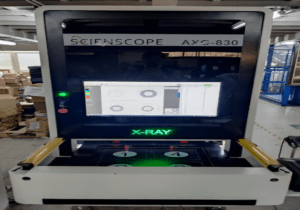
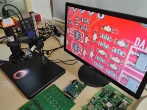
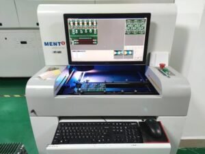
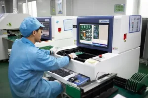
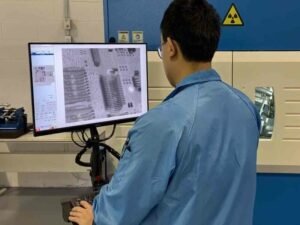
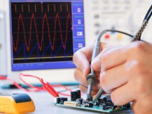
7. Testing and Quality Control
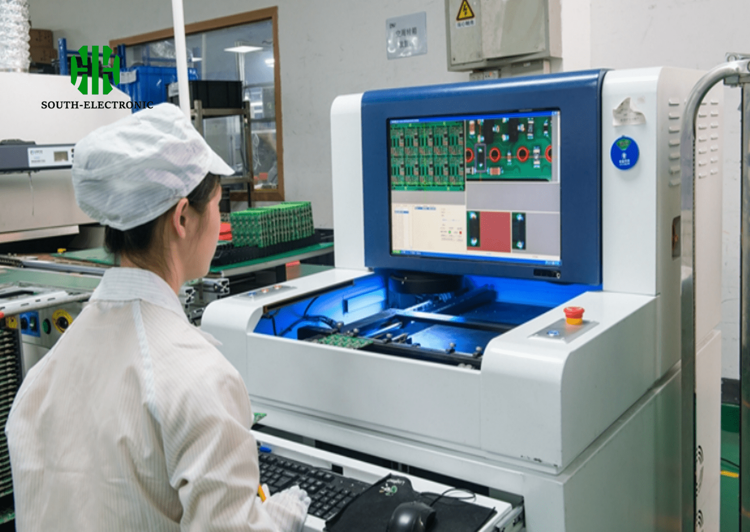
Every PCB we produce goes through extensive testing to make sure it meets the required specifications. We run electrical tests to check for shorts and opens, mechanical tests to evaluate flexibility and durability, and environmental tests to ensure performance under various conditions. Quality control is especially important when it comes to wearable PCBs because these devices often come into direct contact with the user and need to work reliably.
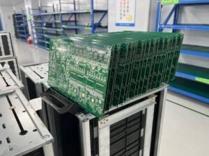
8. Final Assembly and Packaging
Once the PCB pass all tests, they are assembled into the final product or prepared for shipment to the customer for assembly. Packaging for wearable PCB is designed to protect the delicate circuits during transit and ensure that they arrive in perfect condition.
Chapter 7
Power Management in Wearable PCB
Power management is a big deal when you‘’re designing a wearable PCB. These things usually run on batteries, and they‘’re expected to run for a long time. Power management is all about making sure your device runs well and uses as little power as possible, so the battery lasts a long time and the user has a good experience.
1. Choosing and Adding a Battery
Choosing the right battery is key to managing power on wearable PCB. You need a battery that is lightweight, small, and can hold a charge for a long time. Lithium-polymer and lithium-ion batteries are popular choices because they have a lot of energy for their size and can be made into different shapes. This makes them perfect for small wearable devices. Adding the battery to the PCB means you have to think about how to lay everything out so you don‘’t waste space and so everything is safe and works well.
2. Making the Voltage Right
Voltage regulators are used to control the power going to the PCB and its parts. These regulators change the voltage to a steady level that the parts can use without getting hurt. Wearable devices usually use low-dropout (LDO) regulators because they work well when there is only a little difference between the voltage going in and the voltage going out. They are good for low-power devices because they help keep the power that gets turned into heat as low as possible. This is important for wearables because they don‘’t like to get hot.
3. Power Efficient Components
Selecting power-efficient components is essential for reducing the overall energy consumption of wearable PCB. This includes using microcontrollers, sensors, and other components that operate at lower power levels. Manufacturers often opt for components that support sleep modes, where the device can enter a low-power state when not actively in use, significantly extending battery life.
4. Energy Harvesting Techniques
Innovative wearable PCB designs use energy harvesting techniques to extend battery life even more. These techniques involve gathering energy from the environment, such as solar power, thermal gradients, or kinetic energy from body movements. For example, piezoelectric materials can generate power from pressure or bending movements, which is perfect for wearables.
5. Power Management ICs
Power Management Integrated Circuits (PMICs) are used in more complex wearables to efficiently handle various power management tasks. These ICs can control charging and discharging, manage power distribution to different parts of the PCB, and handle multiple power sources. They are crucial for optimizing power consumption across the device’s various operational modes.
6. Power Management Software Optimization
Software is a big part of power management because it controls when and how different parts of the wearable device turn on. By optimizing software algorithms and device firmware, developers can reduce the power used by processes that aren’t critical, schedule tasks efficiently, and manage sensor data collection to use as little energy as possible.
7. Testing and Validation
Testing and validation are key to making sure the power management strategies we put in place are working. This means we need to simulate different usage scenarios to see how the device performs under different conditions and make any adjustments we need to. This is how we make sure the wearable PCB lives up to its promise of long battery life and efficient power use.
In conclusion, it is crucial to have effective power management in wearable PCB. This is because it affects everything from user satisfaction to device functionality. By using advanced hardware solutions, energy-efficient components, and optimizing software, manufacturers can create wearable devices that not only meet, but exceed expectations in terms of performance and power efficiency.
Chapter 8
Wearable PCB in the Market: Case Studies
Introduction to Market Trends in Wearable PCB
Wearable PCB has revolutionized various industries by enabling the integration of technology into everyday life. As demand grows, manufacturers are continually innovating to make these devices more efficient, comfortable, and useful. The following case studies showcase successful applications and the unique challenges they overcame.
1. Fitness Tracking Devices
Case Study: Fitbit Flex Circuit Design The Fitbit Flex represents a significant advancement in fitness tracking technology. Its PCB is exceptionally flexible and thin, designed to fit comfortably around the wrist. The device uses a minimalist approach with a small number of high-efficiency components to maximize battery life. The PCB also features a unique arrangement that allows for an integrated antenna for Bluetooth connectivity, essential for syncing data with smartphones. This design addresses the primary user demand for unobtrusive and continuous fitness tracking without frequent charging.
2. Medical Monitoring Devices
Case Study: Zio Patch by iRhythm The Zio Patch is a cardiac monitoring device that patients wear for up to 14 days to detect irregular heart activities. The wearable PCB inside the Zio Patch is designed for long-term skin contact, using biocompatible materials to minimize skin irritation. It incorporates an ultra-low-power microcontroller and a compact battery, optimized for extended use. The PCB’s design and materials ensure that it can record continuously without interrupting the patient’s daily activities, illustrating the critical role of power management and material selection in medical wearables.
3. Smart Clothing
Case Study: Levi’s Commuter x Jacquard by Google The collaboration between Levi’s and Google brought about a smart jacket that allows users to interact with their devices via touch and gesture-sensitive areas integrated into the fabric. The wearable PCB in this jacket is not only flexible but also washable, designed to withstand the rigors of regular use in clothing. This case study highlights the innovative integration of conductive yarns and miniaturized electronics, pushing the boundaries of what’s possible in wearable tech by merging fashion with functionality.
4. Advanced Prosthetics
Case Study: Advanced Bionic Limbs by Ottobock Ottobock’s bionic limbs use sophisticated wearable PCB to provide users with highly responsive control and natural movement. The PCB in these prosthetics are compact and shaped to fit within the mechanical constraints of artificial limbs. They include sensors and actuators that respond to muscle movements, allowing for smooth and intuitive limb control. This example emphasizes the importance of custom PCB designs in enhancing the quality of life for individuals with disabilities.
5. Child and Elderly Care Monitoring
Case Study: AngelSense GPS Tracker AngelSense is designed to help caregivers monitor the whereabouts and well-being of children and elderly individuals. The wearable PCB used in this device includes GPS functionality and voice communication capabilities. It’s engineered for durability and longevity, featuring power-saving algorithms to extend battery life throughout the day. This case study demonstrates how wearable PCB can be tailored to meet the specific needs of safety and communication in vulnerable populations.
Conclusion
These case studies illustrate the diverse applications of wearable PCB across various market segments, highlighting the specialized requirements and innovative solutions involved in their design and implementation. For companies like South-Electronic, these examples provide valuable insights into the challenges and opportunities in the wearable technology market, guiding future projects and client engagements in creating effective, user-centered wearable devices.
Chapter 9
Future Trends and Innovations in Wearable PCB Technology
Introduction to Emerging Trends
As wearable tech gets more and more integrated into our lives, the PCB design and manufacturing that goes into it is evolving. This evolution is not only making wearables more functional, but it’s also making them more wearable and reliable. Here are some of the trends that are going to drive big changes in the wearable PCB market.
1. Miniaturization and High-Density Integration
Trend Overview: The push towards making devices smaller and more comfortable without sacrificing functionality is driving innovations in miniaturization and high-density component integration. Future wearable PCB is expected to utilize ultra-compact components and multi-layer designs that allow for more sophisticated circuitry in smaller spaces. This trend is critical for devices like smartwatches and fitness bands, where space is at a premium.
Impact on Design and Manufacturing: Manufacturers will need to adopt advanced lithography techniques to handle the increased circuit density. This includes improvements in material science, particularly in substrates that can support tighter trace widths and spaces. Additionally, the use of HDI (High-Density Interconnect) technology will become more prevalent.
2. Flexible and Stretchable Electronics
Trend Overview: The development of flexible and stretchable PCB is set to revolutionize wearable technology. Unlike traditional rigid boards, these flexible circuits can conform to the contours of the human body, offering enhanced comfort and broader application possibilities in clothing and even directly on the skin.
Impact on Design and Manufacturing: This innovation requires new materials and manufacturing processes that can ensure circuit functionality despite bending and stretching. Materials such as liquid crystal polymer (LCP) and new forms of polyimide are being developed to enhance the durability and flexibility of wearable PCB. Techniques like 3D printing of conductive inks are also being explored to create these adaptive circuits.
3. Energy Efficiency and Power Generation
Trend Overview: As wearables are typically limited by battery size, improving energy efficiency remains a priority. Future trends include not only optimizing power consumption through smarter chip design and power management systems but also integrating energy-harvesting technologies that convert body heat, motion, or solar energy into electrical energy.
Impact on Design and Manufacturing: Incorporating energy-harvesting materials and technologies directly into PCB may lead to the development of self-sustaining wearables. Research into nanogenerators, thermoelectric generators, and organic photovoltaics is paving the way for these advancements.
4. Biocompatibility and Health Monitoring
Trend Overview: As wearable devices increasingly monitor health in real-time, the demand for biocompatible materials that can safely interact with the human body is growing. Future wearable PCB will likely incorporate sensors capable of more complex and accurate health diagnostics, from measuring blood oxygen levels to detecting pathogens in the wearer’s environment.
Impact on Design and Manufacturing: Manufacturers will need to ensure that materials used in PCB are hypoallergenic and non-toxic. Additionally, integrating advanced biosensors into PCB will require sophisticated calibration and validation to meet medical standards.
5. AI and Machine Learning Integration
Trend Overview: Integrating AI and machine learning algorithms directly into wearable devices enables more personalized and adaptive user experiences. Future wearable PCB will need to support AI processing capabilities, potentially through embedded AI chips or through edge computing frameworks.
Impact on Design and Manufacturing: This trend will drive the need for PCB with higher processing power and faster data transfer rates. It may also require closer collaboration between hardware engineers and software developers to optimize AI functionalities directly on the device.
Conclusion
The future of wearable PCB technology is marked by rapid advancements in design, materials, and functionality. These trends highlight the industry’s move towards more personalized, energy-efficient, and health-focused devices. For manufacturers and designers, staying ahead means embracing these innovations, investing in new technologies, and continually adapting to the evolving needs of consumers.
Chapter 10
How to Choose the Right Wearable PCB Supplier
Choosing a PCB supplier is a big deal. It can make or break your wearable tech design, production, and overall success. Since wearables are a specialized PCB, you need to evaluate suppliers based on their expertise, technology, and ability to deliver products that meet specific wearable standards.
Step 1: Check Out Their Tech Skills and Industry Experience
First things first: You need to make sure the supplier has the technical chops and industry experience to handle your project. You want a supplier that has a proven track record of manufacturing wearable PCB. These products often require advanced technologies like flexible circuits and high-density interconnects (HDI).
Review Past Projects: Ask for case studies or examples of previous projects similar to yours. This can give you an idea of the supplier’s ability to handle specific requirements for wearable technology, such as small size, flexibility, and durability.
2. Assess Production Quality and Standards
Quality Certifications: Ensure the supplier has the appropriate quality certifications, such as ISO 9001 for quality management systems or ISO 13485 for wearables with medical applications. These certifications show that the supplier follows strict manufacturing standards.
Quality Control Processes: Ask about their quality control processes. Effective quality control measures are essential to producing reliable and durable wearable PCB. This includes testing flexibility and durability, especially when the PCB will bend or move frequently.
3. Consider material and technology options
Advanced materials: Because wearables have special needs, suppliers should have access to and be familiar with advanced materials, like flexible substrates and conductive inks, which are often used in wearable PCB.
Tech chops: Make sure the supplier can handle the latest PCB technologies, like miniaturization and multi-layer printing. This is especially important for wearables, where space and weight are everything.
4. Check scalability and flexibility
Scalability: The supplier should be able to scale production based on your needs. Whether you are starting with a small production run or anticipate rapid growth, the supplier must be able to adapt to changing needs without compromising quality or delivery time.
Flexibility for design changes: Flexibility is key during the development phase of a wearable PCB. Suppliers should be able to accommodate design changes and iterative improvements based on prototype testing and feedback.
5. Analyze lead times and logistics
Lead times: Check out the supplier’s lead times from order to delivery to make sure they match up with your project timeline. If your PCB are late, it can really screw up your product launch and getting into the market.
Shipping and delivery: Get a handle on their shipping capabilities, especially if your market involves global delivery. You need a shipping process that is reliable and efficient to make sure your PCB get to you in one piece and on time.
6. Evaluate communication and customer service
Good communication: Good communication is key when dealing with complex projects like wearable PCB. Suppliers should provide clear, consistent updates and be responsive to any questions or concerns that may come up.
Customer support: See how good the customer support is. Suppliers that offer comprehensive support, from design assistance to post-delivery services, can be a great partner in the lifecycle of your wearable product.
7. Compare costs and value propositions
Cost considerations: While cost should not be the only determining factor, it is important to compare pricing between suppliers to ensure you are getting good value. Consider the total cost, including production, shipping, and any additional charges for design changes or rush orders.
Value-added services: Some suppliers may offer additional services, such as design optimization, prototyping, and even end-to-end assembly. These can provide added value and should be considered when making your selection.
Conclusion
When choosing a wearable PCB supplier, you need to evaluate their capabilities, quality standards, technical capabilities, and their ability to meet your specific project needs. By carefully considering these factors, you can establish a partnership that will improve the quality and success of your wearable technology products. This comprehensive approach ensures that the supplier you choose will not only meet your expectations, but may exceed them in terms of providing high-quality wearable PCB.
Get in touch
Where Are We?
Industrial Park, No. 438 Donghuan Road, No. 438, Shajing Donghuan Road, Bao'an District, Shenzhen, Guangdong, China
Floor 4, Zhihui Creative Building, No.2005 Xihuan Road, Shajing, Baoan District, Shenzhen, China
ROOM A1-13,FLOOR 3,YEE LIM INDUSTRIAL CENTRE 2-28 KWAI LOK STREET, KWAI CHUNG HK
service@southelectronicpcb.com
Phone : +86 400 878 3488
Send us a message
The more detailed you fill out, the faster we can move to the next step.


