
Do your PCB designs fail reliability tests? Poor post-drilling processes might silently sabotage signal quality and connectivity. Don’t risk product failures when simple steps can prevent costly errors.
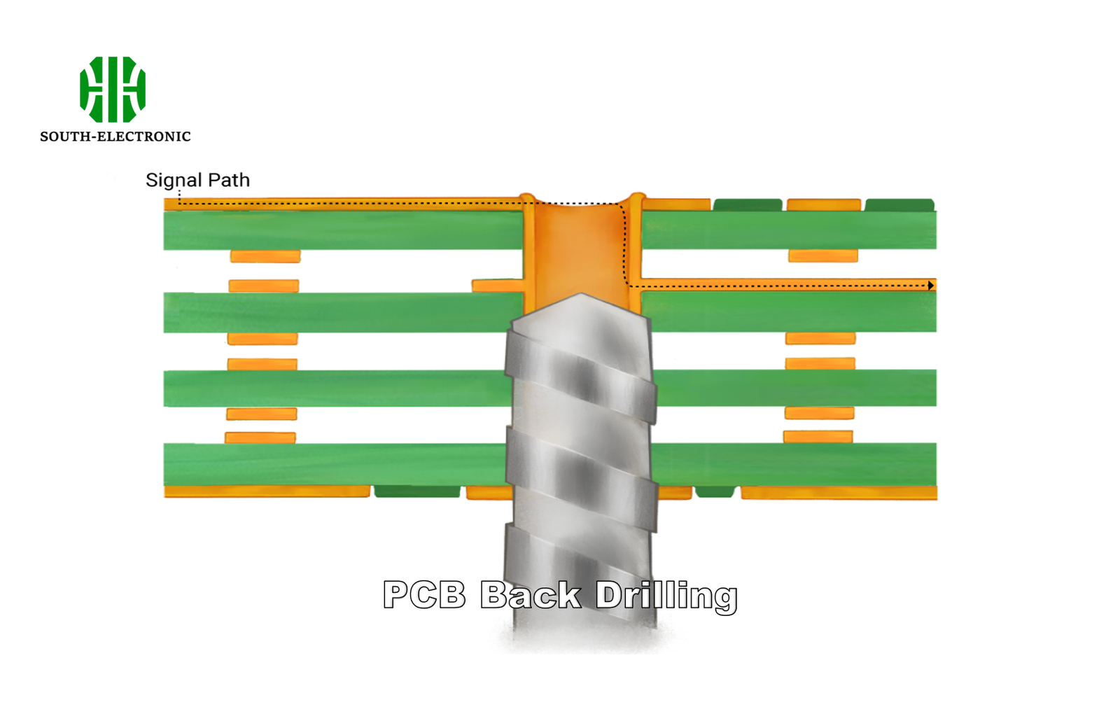
PCB post-drilling processes include deburring to remove copper burrs, desmearing to eliminate epoxy residue, and back-drilling to improve signal integrity. These essential steps clean and prepare hole walls for plating, ensuring reliable electrical connections in multilayered boards.

Understanding these foundational processes helps you avoid manufacturing defects. Now explore the specific challenges affecting drilling outcomes in modern electronics.
What are the key factors affecting PCB drilling accuracy?
Ever wasted boards due to misaligned holes? Drilling accuracy depends on several interacting factors many engineers overlook. Recognize these variables to optimize your fabrication process.
Drilling precision hinges primarily on machine stability, tool condition, material characteristics, and process parameters like feed rate. Controlling these variables prevents unwanted hole position deviations and ensures proper layer registration.
Why Drilling Parameters Matter
PCB drilling isn’t just about punching holes. Critical variables affect whether holes hit their targets accurately. Material composition comes first – harder substrates require specific drill bits. Machine calibration is equally vital; regular checks prevent position drift. Drill wear causes diameter variations as tools dull after multiple holes.
Environmental considerations also impact results. Temperature fluctuations expand boards marginally while humidity swells fiberglass. Cleanliness matters too; dust accumulation shifts drill positions. Balancing all elements maintains consistent registration.
| Factor | Impact | Control Method |
|---|---|---|
| Drill Bit Wear | Hole size reduction ±0.02mm | Replace after 300-500 hits |
| Spindle Speed | Burr formation | Maintain 60,000-120,000 RPM range |
| Feed Rate | Drill flex/breakage | Apply 1.5-6m/min matching material |
| Material Type | Tool degradation | Diamond-coated drills for ceramics |
| Temperature | Board expansion | ±2°C workshop control |
I once faced a prototype disaster from ignoring drill wear checks. When we instituted scheduled bit replacements, hole alignment improved by 27%.
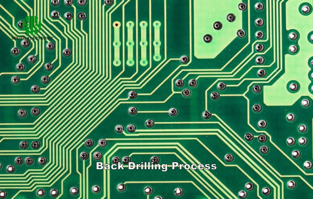
What are the common defects in PCB drilling hole wall quality?
Seeing plating voids after manufacturing? Hole wall defects often originate from incorrect drilling practices. Spotting these issues early prevents electrical failures in final assemblies.
Major drilling defects include nail heading (tapered holes), resin smear (epoxy residue), and wedge voids (fractured walls). These imperfections inhibit copper plating, creating reliability risks for high-frequency applications.
Addressing Material Fracture Mechanisms
Hole quality defects stem from physical interactions between drills and composite laminates. Resin smear happens when heat during drilling melts epoxy, coating copper layers – subsequent desmearing is mandatory. Nail heading occurs when exits widen, causing hourglass-shaped holes that weaken plating.
Wedge voids form differently. Brittle prepreg layers fracture rather than cut cleanly, leaving micro-cracks. Roughness often follows as glass fibers tear instead of shearing. These conditions enable acid traps during etching.
| Defect | Cause | Solution |
|---|---|---|
| Smear | Excessive drilling heat | Proper RPM/feed rate adjustments |
| Nail Heading | Tool vibration on exit | Support material with backup boards |
| Roughness | Dull drill bits | Sharper tools + entry/exit materials |
| Voiding | Delamination forces | Optimized stack-up clamping |
| Taper | Drill deflection | Stiffer drill tools (carbide alloy) |
Through-hole void rejection rates dropped from 12% to 3% when we adopted diamond-coated drills. Material testing proved fewer glass-fiber pullouts.
When to choose mechanical vs. laser drilling for PCBs?
Choosing wrong drilling methods increases costs unnecessarily. Each technology serves specific design requirements better. Match your hole specifications to the process to optimize both performance and budget.
Select mechanical drilling for standard holes above 0.15mm diameter and high-volume production. Use laser drilling for micro-vias under 0.1mm, complex shapes, or when processing brittle ceramic substrates requiring non-contact methods.
Micro-Via Evolution Needs Hybrid Approaches
The choice isn’t binary – modern HDI boards often use both methods strategically. Mechanical drilling dominates cost efficiency for conventional holes. Its rotating cutters handle copper-clad boards effectively. But limitations emerge with miniaturization; spindles physically can’t handle <0.15mm holes reliably.
Laser ablation solves micro-scale needs, especially for blind/buried vias. CO₂ lasers process organics quickly, while UV lasers achieve sharper ceramic cuts. However, conductive debris requires extra cleaning steps. Consider these parameters:
| Criteria | Mechanical | Laser |
|---|---|---|
| Min Hole Size | 0.15mm | 0.05mm |
| Material Flex | Limited by hardness | Handles ceramics/metal |
| Setup Speed | 30-60 min | Minutes |
| Ongoing Cost | Drill bits ($10-$100 each) | Laser maintenance ($2000/yr) |
| Accuracy | Up to ±0.025mm | Up to ±0.005mm |
| Production Rate | 700 holes/min | 200 holes/min |
I switched to laser drilling for mobile sensor boards after mechanical tools broke on 0.08mm holes. This reduced waste rates by 40% overnight.
Conclusion
Master PCB drilling through controlled parameters and defect prevention while strategically choosing mechanical or laser methods based on hole specs for reliable, high-performance boards.

