
Have you spent weeks designing electronics only to realize your circuit board lacks stability? This frustration happens when materials get overlooked. Let me share how rigid PCBs are built to endure tough conditions.
Rigid PCBs primarily consist of a solid FR-4 substrate layer bonded to conductive copper foil, topped with protective solder mask and silkscreen markings. This 4-layer sandwich creates a rigid backbone that prevents bending while ensuring reliable electrical connections – perfect for devices needing structural integrity.
Now that you understand their core composition, let’s tackle common manufacturing challenges you might face with rigid boards. These practical solutions will save time and money.
How can I get rigid PCBs made cheaper?
Stressed about PCB costs wrecking your project budget? Unexpected price hikes often delay hardware launches. Here are proven methods to reduce expenses without quality loss.
Optimize board size specifications, use standard FR-4 materials, increase order quantities for bulk discounts, and simplify designs to lower rigid PCB manufacturing costs by 15-30% while keeping reliability.

Strategic Cost Analysis Table
| Cost Factor | Cheap Approach | Premium Approach | Savings Impact |
|---|---|---|---|
| Board Size | Compact layouts | Large panels | High (30-50%) |
| Layers | 1-2 layers | 4+ layers | Medium (20-40%) |
| Material | Standard FR-4 | Specialty laminates | High (25-45%) |
| Quantity | Bulk orders | Small batches | Medium (15-35%) |
| Finishing | Lead-free HASL | Gold plating | Low (10-20%) |
Every design choice influences pricing. I found reducing unused board area through efficient component placement immediately cuts material waste. Bulk production yields the most savings – consolidating three projects into one order saved me 28% last quarter. Standard green solder masks are cheaper than exotic colors. Remember: connect with multiple manufacturers early. Their moq discounts often surprise newcomers. However, never compromise on core copper thickness; below 1oz risks reliability. Balance savings with durability requirements.
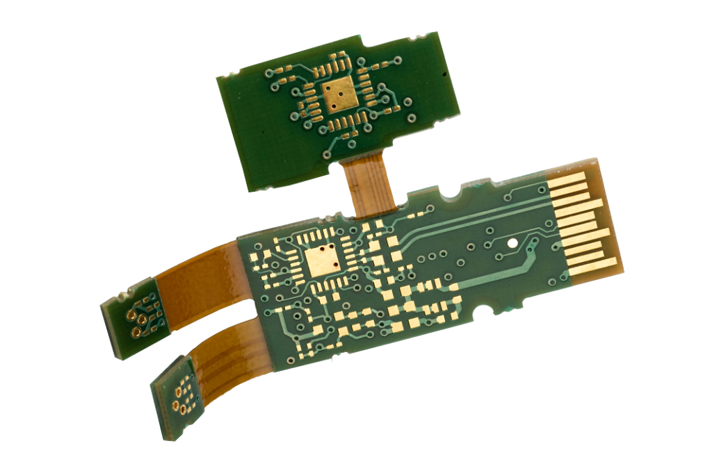
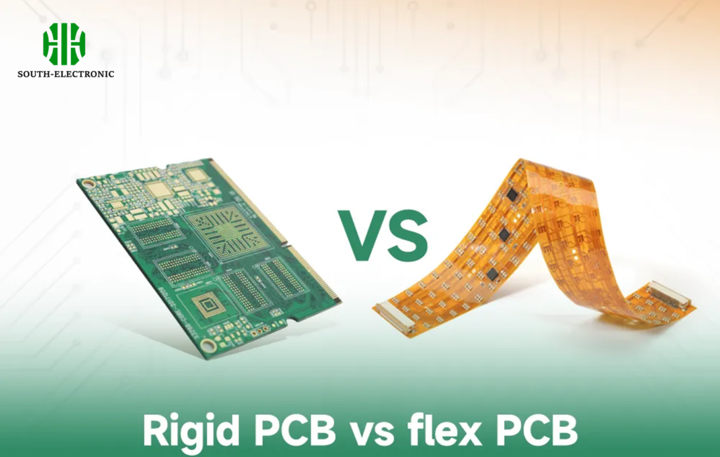
Rigid PCB or rigid-flex PCB: Which one’s right for me?
Struggling to choose between rigid and bendable solutions? This common dilemma causes expensive redesigns when projects evolve unexpectedly. Clear use-case analysis prevents this pain.
Select rigid PCBs for stationary electronics needing cost efficiency and maximum durability, while rigid-flex variants suit dynamic products requiring 3D shaping like wearable tech or folding gadgets.
Decision Matrix Breakdown
| Design Aspect | Rigid PCB | Rigid-Flex PCB |
|---|---|---|
| Cost | Low ($) | High ($$$) |
| Durability | Excellent | Moderate |
| Shape Flexibility | None | Excellent |
| Weight | Standard | Lightweight |
| Installation Space | Fixed-space | Variable-space |
Rigid PCBs serve most static applications best. Their solid construction suits power supplies or computer motherboards that experience high thermal stress. When testing consumer gadgets, I choose rigid options for prototype stages to validate circuits affordably before investing in flexible tech. Consider environmental factors too: vibration-heavy or moisture-prone deployments demand rigid PCBs’ robust nature. However, if your drone needs folded circuits inside wings or a medical device contours to body curves, hybrid rigid-flex solves that. But remember: complex multilayer flex designs increase costs threefold. Always match the board to physical demands.
How do I design a rigid PCB for high-speed signals?
Facing signal distortion issues in GHz-range circuits? Digital noise from poor layouts often corrupts critical data. I’ll explain how to preserve integrity.
Design rigid PCBs for high-speed signals using impedance-controlled traces, nearby ground planes, minimized via usage, and quality dielectric materials to prevent crosstalk and losses above 100MHz.

Design Parameter Optimization
| Critical Factor | Standard Design | High-Speed Design | Why Important |
|---|---|---|---|
| Trace Width | Uncontrolled | Calculated precision | Impedance stability |
| Dielectric Constant | FR-4 standard | Low-Dk materials | Signal propagation |
| Grounding | Partial planes | Continuous layers | Noise absorption |
| Trace Lengths | Variable | Matched pairs | Signal synchronization |
| Via Count | Unlimited | Minimal (1GHz. Beware: more than 8 signal layers need careful stack-up analysis. The ground plane must be unbroken beneath critical traces; I’ve fixed timing errors simply by adding copper fills. Each bend increases reflection risks – smooth 45° corners outperform harsh right angles. Finally, test with VNA equipment when prototyping. |
Conclusion
Understanding rigid PCB materials and design principles transforms electronics projects. Apply these proven strategies to optimize costs, select formats, and master signal integrity efficiently.

