
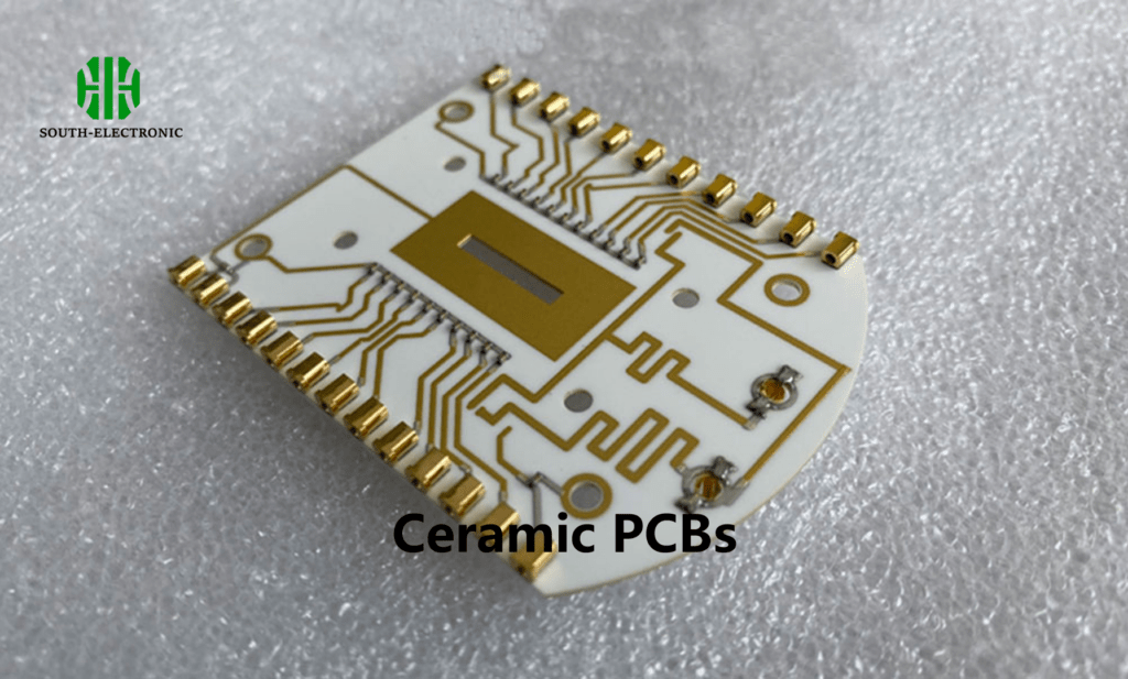
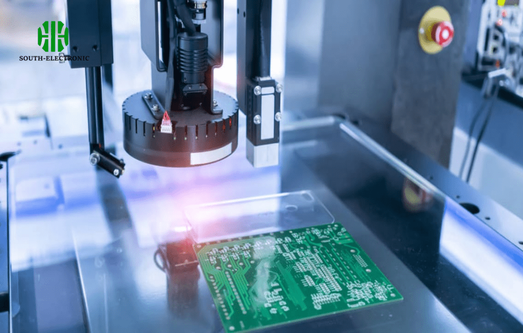
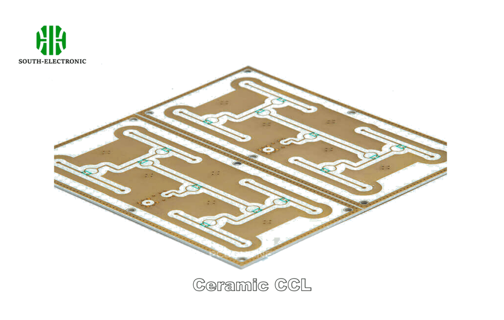
Ceramic substrates are specially crafted boards in which copper foil is directly bonded to the surface (one or both sides) of an alumina (Al2O3) or aluminum nitride (AlN) ceramic substrate at high temperatures. The resulting ultra-thin composite substrate exhibits excellent electrical insulation, high thermal conductivity, superior solderability, and high adhesion strength. Similar to PCBs, it can be etched with various patterns and possesses a high current-carrying capacity. Therefore, ceramic substrates have become a fundamental material for high-power power electronics circuit structure and interconnection technologies.
The advent of ceramic substrates has ushered in new developments in the heat dissipation application industry. Due to their heat dissipation characteristics, coupled with their advantages such as high heat dissipation, low thermal resistance, long life, and high voltage resistance, improvements in production technology and equipment have led to accelerated price reductions, expanding the application areas of the LED industry, such as indicator lights in home appliances, automotive lights, streetlights, and large outdoor billboards. The successful development of ceramic substrates has provided better services for indoor and outdoor lighting products, broadening the future market for the LED industry.
What are the characteristics of ceramic substrate PCBs?
- 1.Strong mechanical stress resistance and stable shape; high strength, high thermal conductivity, and high insulation; strong bonding and corrosion resistance.
- 2.Excellent thermal cycling performance, with up to 50,000 cycles and high reliability.
- 3.Can be etched into various patterns and structures, similar to PCBs (or IMS substrates); pollution-free and harmless.
- 4.Wide operating temperature range -55°C to 850°C; thermal expansion coefficient close to silicon, simplifying the production process of power modules.
Common Ceramic Substrate Materials
- Alumina (Al2O3)
Alumina substrates are the most commonly used substrate material in the electronics industry. Their mechanical, thermal, and electrical properties are superior to most other oxide ceramics; their strength and chemical stability are superior, and their abundant raw material resources make them suitable for a wide range of manufacturing technologies and shapes. Sliton’s alumina substrates are now available for 3D customization.
- Beryllium Oxide (BeO)
It has a higher thermal conductivity than metallic aluminum and is used in applications requiring high thermal conductivity. However, its performance decreases rapidly above 300°C. Most importantly, its toxicity limits its development.
Beryllium oxide ceramics are ceramics primarily composed of beryllium oxide. They are primarily used as substrates for large-scale integrated circuits, high-power gas laser tubes, heat sinks for transistors, microwave output windows, and neutron moderators. Pure beryllium oxide (BeO) is a cubic crystal with a density of 3.03 g/cm³. Its melting point is 2570°C and it exhibits very high thermal conductivity, almost equivalent to that of copper and pure aluminum. Its thermal conductivity coefficient, λ, is 200-250 W/(m.K). It also has excellent thermal shock resistance. Its dielectric constant is 6-7 (at 0.1 MHz) and its dielectric loss tangent is approximately 4 × 10⁻4 (at 0.1 GHz). Its major drawback is that the powder is highly toxic and can cause wounds to heal with contact. Beryllium oxide powder is used as the raw material, and aluminum oxide and other ingredients are added and sintered at high temperatures. Manufacturing this ceramic requires excellent protective measures. Beryllium oxide becomes more volatile in high-temperature media containing moisture, starting to volatilize at 1000°C and increasing in volume with increasing temperature. This creates production difficulties, and some countries no longer produce it. However, despite its high price, the product’s excellent performance still generates considerable demand.
- Aluminum Nitride (AlN)
AlN has two key properties worth noting: high thermal conductivity and a coefficient of expansion that matches that of silicon. However, even a very thin oxide layer on the surface can affect thermal conductivity. Producing AlN substrates with consistent quality requires strict control of materials and processes. Very few domestic companies, like Slitong, are capable of large-scale AlN production. Compared to Al2O3, AlN is significantly more expensive, a bottleneck that has hindered its development. However, with economic growth and technological advancements, this bottleneck will eventually disappear.
Taking all of the above into account, it can be seen that alumina ceramics, due to their superior overall performance, continue to dominate and are widely used in fields such as microelectronics, power electronics, hybrid microelectronics, and power modules.
AlN is stable up to 2200°C. It has high room temperature strength, and its strength decreases slowly with increasing temperature. It has good thermal conductivity and a low thermal expansion coefficient, making it an excellent material for thermal shock resistance. It is highly resistant to molten metal corrosion, making it an ideal crucible material for casting pure iron, aluminum, or aluminum alloys. Aluminum nitride is also an electrical insulator with excellent dielectric properties, making it a promising material for use in electrical components. An aluminum nitride coating on the surface of gallium arsenide protects it from ion implantation during annealing.
Aluminum nitride is also a catalyst for the conversion of hexagonal boron nitride to cubic boron nitride. It reacts slowly with water at room temperature. It can be synthesized from aluminum powder in an ammonia or nitrogen atmosphere at 800-1000°C, resulting in a white to gray-blue powder. Alternatively, it can be synthesized from an Al₂O₃-C-N₂ system at 1600-1750°C, resulting in an off-white powder. Or it can be produced by the vapor phase reaction of aluminum chloride and ammonia. The coating can be synthesized using the AlCl₃-NH₃ system via vapor phase deposition.
- Silicon Nitride (Si₃N₄)
In 2012, Rogers Corporation launched the new curamik® series of silicon nitride (Si₃N₄) ceramic substrates. Because silicon nitride offers higher mechanical strength than other ceramics, the new curamik® substrates help designers achieve the long lifespan crucial for harsh operating environments and HEV/EV and other renewable energy applications.
The new ceramic substrates made of silicon nitride exhibit higher flexural strength than substrates made with Al₂O₃ and AlN. The fracture toughness of Si₃N₄ even exceeds that of zirconia-doped ceramics.
Common Ceramic Substrate Manufacturing Processes
Currently, the five most common types of ceramic heat sink substrates are HTCC, LTCC, DBC, DPC, and LAM. LAM is a patented technology developed by Slitron in collaboration with the National Laboratory for Optoelectronics at Huazhong University of Science and Technology. Both HTCC and LTCC use sintering processes, resulting in higher costs. DBC and DPC are specialized technologies that have only recently matured and reached mass production in China. DBC utilizes high-temperature heating to bond Al2O3 to a Cu substrate. However, the technical bottleneck is the difficulty in resolving the micropores between the Al2O3 and Cu substrates, which significantly challenges the mass production capacity and yield of this product. DPC, on the other hand, utilizes direct copper plating to deposit Cu onto an Al2O3 substrate. This process combines material and thin-film processing technologies, resulting in products that have become the most commonly used ceramic heat sink substrates in recent years. However, the high level of material control and process integration required makes the entry into the DPC industry and achieving stable production relatively high. LAM technology is also known as laser-activated metallization.
- HTCC (High-Temperature Co-fired Ceramic)
HTCC, also known as high-temperature co-fired multilayer ceramic, has a manufacturing process very similar to LTCC. The main difference is that HTCC’s ceramic powder does not contain glass. Therefore, HTCC must be dried and hardened at a high temperature of 1300-1600°C to form a green body. Vias are then drilled, filled, and printed using screen printing. The higher co-firing temperature limits the choice of metal conductor materials. Metals with higher melting points but lower conductivity, such as tungsten, molybdenum, and manganese, are typically used. Finally, the layers are sintered together to form the finished product.
- LTCC (Low-Temperature Co-fired Ceramic)
LTCC, also known as low-temperature co-fired multilayer ceramic substrate, is a process that involves mixing inorganic alumina powder with approximately 30%-50% glass material and an organic binder to create a slurry. The slurry is then scraped into sheets using a scraper. After a drying process, the sheets are formed into thin green sheets. Vias are then drilled according to the design of each layer to transmit signals. Internal circuitry within the LTCC is screen-printed, filling the holes and printing circuits on the green sheets. Internal and external electrodes can be made of metals such as silver, copper, and gold. Finally, the layers are laminated and sintered in a sintering furnace at 850-900°C to complete the process.
- DBC (Direct Bonded Copper)
Direct copper bonding technology utilizes copper’s oxygen-containing eutectic solution to bond copper directly to ceramic. The basic principle is to introduce an appropriate amount of oxygen between the copper and ceramic before or during the bonding process. Within the temperature range of 1065°C to 1083°C, copper and oxygen form a Cu-O eutectic solution. DBC technology utilizes this eutectic solution to chemically react with the ceramic substrate to form a CuAlO₂ or CuAl₂O₄ phase, while also wetting the copper foil to achieve a bond between the ceramic and copper substrates.
What are the advantages of ceramic substrate PCBs?
- ◆ The thermal expansion coefficient of ceramic substrates is close to that of silicon chips, eliminating the need for transition layer Mo sheets, saving labor, materials, and costs.
- ◆ Reducing solder layers reduces thermal resistance, reduces voids, and improves yield.
- ◆ At the same current carrying capacity, the trace width of 0.3mm thick copper foil is only 10% that of a typical printed circuit board.
- ◆ Excellent thermal conductivity enables very compact chip packaging, significantly increasing power density and improving system and device reliability.
- ◆ Ultra-thin (0.25mm) ceramic substrates can replace BeO without environmental toxicity issues.
- ◆ High current carrying capacity: a continuous current of 100A flowing through a 1mm wide, 0.3mm thick copper conductor results in a temperature rise of approximately 17°C; a continuous current of 100A flowing through a 2mm wide, 0.3mm thick copper conductor results in a temperature rise of only approximately 5°C.
- ◆ Low thermal resistance: the thermal resistance of a 10×10mm ceramic substrate is 0.31K/W for a 0.63mm thick ceramic substrate. The thermal resistance of a 0.38mm thick ceramic substrate is 0.19K/W, and that of a 0.25mm thick ceramic substrate is 0.14K/W.
- ◆ High insulation withstand voltage, ensuring personal safety and equipment protection.
- ◆ Enables new packaging and assembly methods, enabling highly integrated products and reducing size.
What are the uses of ceramic substrate PCBs?
◆ High-power power semiconductor modules; semiconductor coolers, electronic heaters; RF power control circuits, power hybrid circuits.
◆ Intelligent power components; high-frequency switching power supplies, solid-state relays.
◆ Automotive electronics, aerospace, and military electronic components.
◆ Solar panel assemblies; telecommunications dedicated switches, receiving systems; lasers and other industrial electronics.
The advent of ceramic substrates has sparked the development of the heat dissipation application industry. Due to their heat dissipation characteristics, coupled with their advantages such as high heat dissipation, low thermal resistance, long life, and voltage resistance, improvements in production technology and equipment have led to a rapid price rationalization, further expanding the LED industry’s application areas, such as indicator lights in home appliances, automotive lights, streetlights, and large outdoor billboards. The successful development of ceramic substrates will further expand the LED industry’s future market by providing services for indoor and outdoor lighting products.


