
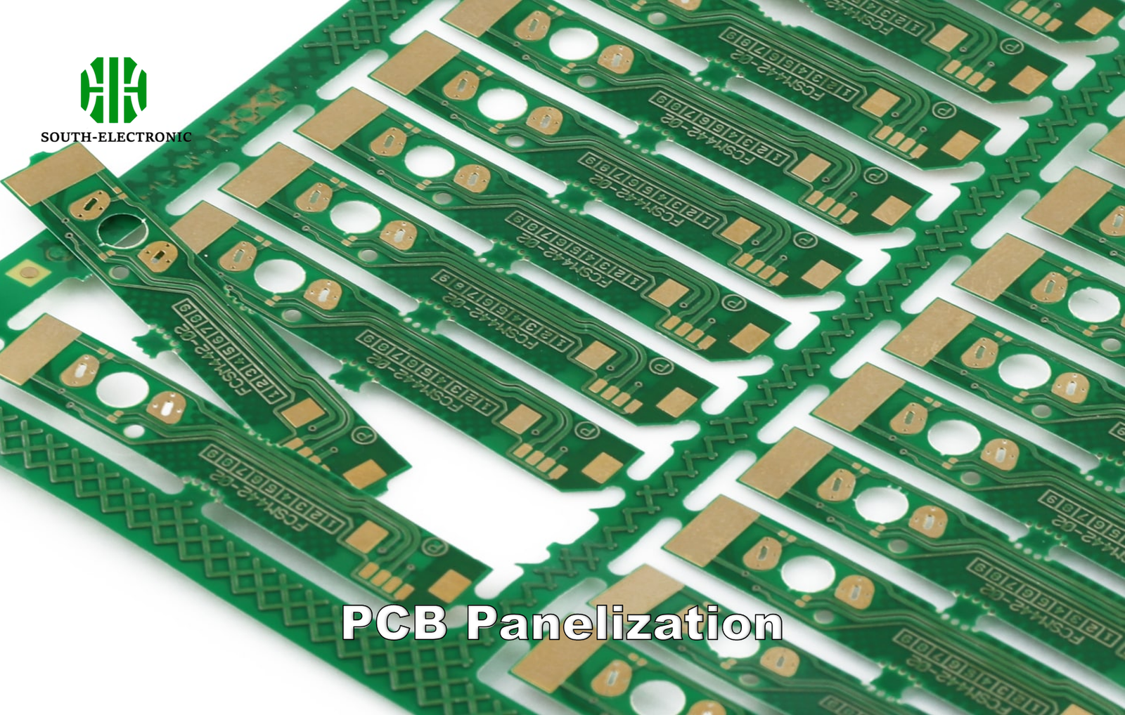
Creating custom electronics? You’re probably burning money and time right now. Proper PCB panel sizing fixes that.
Standard sizes like 18"x24", 18"x12", and 9"x24" (or 460mmx610mm/457mmx610mm) fit most equipment, slash waste by 15-30%, and cut your manufacturing costs. These dimensions balance factory compatibility with material efficiency, though always verify specifics with your fab house.
Think your board shape or size is too unique? Stick with standards. What really drives your costs and assembly success might surprise you—let’s break it down.
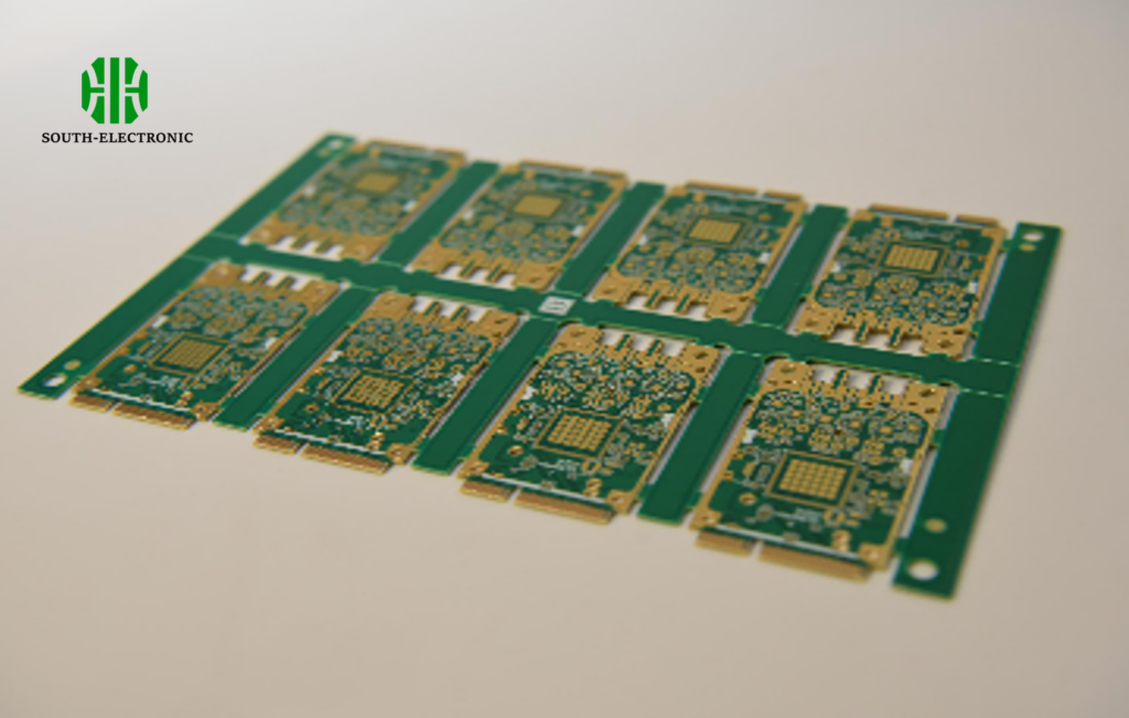
V-Score vs Breakaway Tab: Which PCB Panel Depanelization Method is Right for Your Design?
Your boards are panelized—but separating them risks cracks and lost components. Choosing wrong costs thousands in rejects.
V-score cuts grooves for clean snaps in straight-line boards but stresses components near edges. Breakaway tabs use drilled holes for complex shapes and dense components but leave nubs requiring manual removal. Match method to your board geometry and component density.

Why Depanelization Choice Dictates Failure Rates
Poor separation methods account for 22% of SMT assembly defects. Both techniques solve specific problems:
| Factor | V-Score | Breakaway Tabs |
|---|---|---|
| Best For | Rectangular boards | Irregular shapes |
| Stress on PCB | High (crack risk near grooves) | Low (if holes positioned well) |
| Post-Production | No cleanup needed | Requires manual de-burring |
| Component Safety | Avoid near scored edges | Safe for nearby components |
| Cost Impact | Lower tooling cost | Higher labor for removal |
V-scores work fastest for simple designs like LED strips. I once saw a drone controller ruined by v-scores placed under MEMS sensors—vibration cracked every unit. Tabs saved a medical device with odd angles, but added $0.17/unit deburring. For dense BGAs, neither works; laser depaneling avoids stress entirely but doubles tooling fees. Always simulate stresses in your CAD tool first.
What Key Factors Affect the Cost of Your PCB Panel (Beyond Board Size)?
Panel invoice 30% higher than expected? Size is just the opener—real costs hide in production details.
**Material utilization efficiency, layer counts, and specialty finishes like ENIG or immersion silver dominate costs. Tight tolerances (85% to avoid "empty space tax."
-
Copper Weight & Layers
2 oz copper doubles foil cost versus 1 oz. Every additional layer adds ~7-12% (e.g., 6L vs 4L). High-Tg materials? Add 15%. -
Finish & Testing
ENIG adds $0.25-$0.50 per board vs HASL. Flying probe testing for complex boards costs more than AOI. One client saved $4700/run by switching from Au plating to ENEPIG on RF boards.
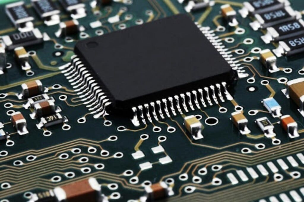
How Does PCB Panel Design Impact SMT Assembly Efficiency and Quality?
Slow SMT lines? Faulty solder joints? Your panel design might be sabotaging production.
Poor fiducial placement or insufficient tooling holes cause misalignment—increasing solder voids by up to 60%. Dense panels lacking clearance spaces invite nozzle crashes, while uneven copper distribution causes temperature drift during reflow.
Engineering for Pick-and-Place Dominance
SMT machines demand harmony between panel design and process. Optimize three zones:
1. Fiducial Strategy
Place 3 global fiducials (≥1mm diameter) near corners. Add local ones for BGAs. Missing these forces vision systems to "guess," creating placement errors up to 0.3mm.
2. Clearance Zones
Leave 5mm clearance on panel edges for clamps. Component-free border areas prevent nozzle strikes during high-speed placements (>25k CPH).
3. Thermal Mass Balance
Large copper pours near small boards cause uneven reflow. One telecom client solved cold joints by adding thieving pads to balance heat absorption—defect rates dropped 18%.
I redesigned an automotive panel by rotating boards 15°, cutting placement time by 11s/panel. Always optimize before locking design.
Conclusion
Standard panel sizes save time and money, but pairing them with smart depanelization, cost-aware specs, and SMT-friendly design completes the efficiency picture. Start with 18"x24".

