
Discovering PCB failures after manufacturing feels frustrating and costly. I know this pain well. Defective boards delay shipments and anger customers. This article reveals practical solutions through key test methods.
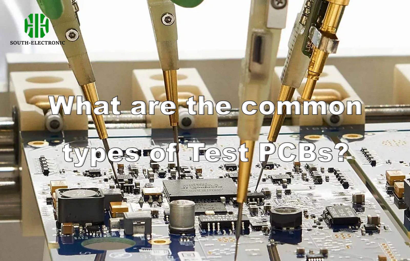
Common test PCB types include In-Circuit Testing (ICT)[^1], Flying Probe Testing[^2], Functional Testing[^3], Automated Optical Inspection (AOI)[^4], Boundary Scan Testing[^5], Burn-In Testing[^6], and X-ray inspection[^7]. Each targets specific defects like short circuits, component failures, or soldering issues during production.
Knowing these test types is just the beginning. Their effectiveness depends on design quality, measurement skills, and cost awareness. I’ll guide you through these critical aspects next.
How to design a reliable Test PCB?
Faulty test designs waste time and money. You might miss critical defects. I’ve faced this headache. Here’s how to create low-risk Test PCBs that deliver accurate results.
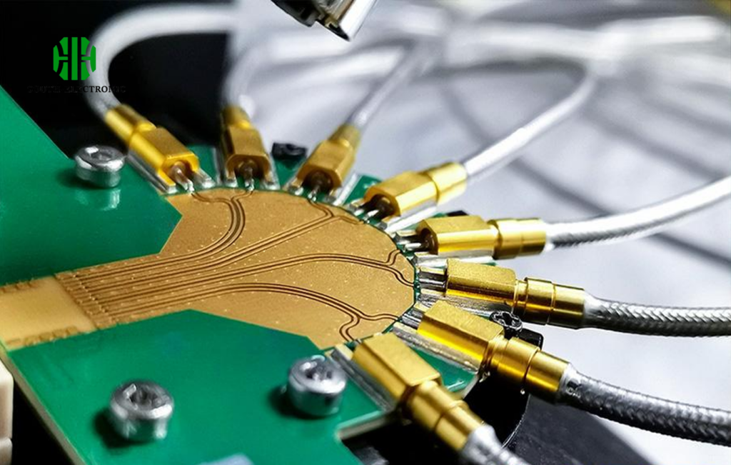
Design reliable Test PCBs by ensuring proper test point placement on critical networks, maintaining clearance rules, and validating trace accessibility. Follow IPC-9252 testability standards. Choose fixtures compatible with your pcb board testing equipment for consistent quality.

Three Pillars of Foolproof Test PCB Design
A well-designed Test PCB needs careful planning in these areas to prevent misdiagnosis during validation:
Strategic Test Point Placement
Place test points on both sides of boards near high-risk components. Each point needs:
- 35 mil minimum pad size
- 100 mil clearance from tall components
- Clear silkscreen labeling
Without these, probes miss connections and yield false passes.
Material and Stackup Considerations
I prioritize materials based on test frequency:
- >10k tests: FR4 with 2oz copper
- High-frequency: Rogers substrates
Imbalanced layer stacks create ghost signals that contaminate measurements.
| Design Element | Pitfall | Solution |
|---|---|---|
| Test point density | Clustered points cause probe collision | Distribute points in grid pattern |
| Fixture access | Hidden test points under components | Reserve 0.5" clearance zones |
| Signal isolation | Crosstalk during boundary scan | Guard traces between high-speed lines |
Maintaining Signal Integrity
During test pcb keyboard validations, noise ruins measurements. My solution: separate analog and digital sections with moats. Use 50Ω impedance matching on RF lines. Implement Kelvin connections at pcb test point locations. I include sacrificial vias to reduce pad cratering during repeated probing.
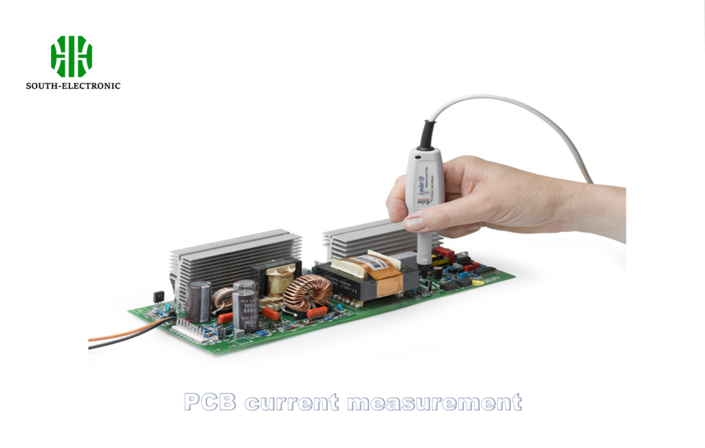
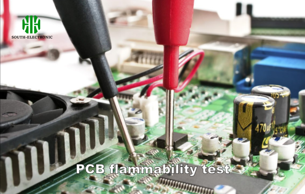
How to measure PCB with a multimeter?
Seeing anomalous readings can confuse anyone. I remember misdiagnosing an open circuit once as a short. Let’s prevent your multimeter frustrations with clear troubleshooting steps.
Use a multimeter to measure PCB continuity, resistance, voltages, and component values. Power off boards for resistance checks. Verify ground connections first. Set multimeter to auto-range mode to prevent wrong readings near low test pcb thresholds.
Accurate Multimeter Methodology
Getting trustworthy results involves understanding measurement contexts and common pitfalls:
Continuity & Resistance Checks
Check continuity with power disconnected. I probe test points back to ground – any >1Ω reading indicates opens. For resistance:
- Discharge capacitors first
- Isolate components during measurement
- Confirm values against schematics
In-circuit measurements often distort values due to parallel paths.
Voltage Measurement Protocol
My 4-step voltage process:
- Confirm meter voltage rating exceeds PCB power
- Connect black probe to verified ground
- Power up board
- Touch test points with red probe
Observe polarity – reversed probes damage meters!
| Measurement | Common Errors | Diagnostic Tips |
|---|---|---|
| Continuity | Testing powered boards | Power OFF – look for beeps under 30Ω |
| Voltage | Floating grounds | Probe ground directly, not chassis |
| Resistance | Residual charge | Discharge capacitors with resistor first |
Critical Component Checks
Transistors and diodes fail frequently – test with diode mode. MOSFETs require gate stimulation measurements. Always handle ICs statically when probing behind the test pcb keyboard interface. For prototype checks, I log all measurements and compare against BOM tolerances.
What factors affect Test PCB costs?
Blaming budget overruns? I once underestimated boundary scan costs by 40%. Test expenses hide under three main variables you must analyze.
PCB test costs change with design complexity, product volumes, chosen test methods, equipment investments, and regulatory standards. Test depth drives cost most – adding pcb testing standards like Class 3 aerospace doubles expenses versus basic validations.
Balancing Economics and Effectiveness
Let’s dissect how testing needs influence budgets at different production stages:
Upfront Development Expenses
Initial costs include:
- Fixture development ($3k-$15k)
- Test programming labor
- Equipment setup
Debugging consumes 30% of this phase. I reduce it through virtual testing before building physical rigs.
Volume-Based Cost Drivers
Cost per test drops sharply after 1000 units. But I add burn-in testing for reliability-critical products like medical devices requiring pcb test blood analyses. Every additional test strategy like AOI+X-ray adds 12-18% to cost.
| Cost Factor | Low-Cost Approach | Quality Tradeoff |
|---|---|---|
| Test Coverage | Flying probe only | Misses parametric faults |
| Fixture Type | Generic springs | Lower uptime than schmoot probes |
| Standards | Self-declared compliance | Risks audit failures versus IPC-610 |
Hidden Operational Expenses
For enterprise executions, download pcb testing methods pdf guides to predict:
- Equipment maintenance fees (8-15%/year)
- Calibration costs (every 2k testing hours)
- Retest percentages from false failures
I include margin-of-error buffers above quoted material costs to absorb these.
Conclusion
Test PCBs need method-specific approaches like ICT for production and multimeters for field diagnostics. Smart designs, precise measurements, and cost-aware planning prevent defects while keeping quality high.
[^1]: Explore this link to understand how ICT can enhance your PCB testing process and improve defect detection.
[^2]: Learn about Flying Probe Testing to see how it can save time and costs in PCB testing.
[^3]: Discover the importance of Functional Testing in ensuring your PCB operates as intended.
[^4]: Find out how AOI can significantly improve the quality control of your PCB manufacturing.
[^5]: Explore this resource to understand how Boundary Scan Testing can help identify defects in complex PCBs.
[^6]: Learn about Burn-In Testing to ensure the reliability of your critical PCB components.
[^7]: Discover how X-ray inspection can reveal hidden defects in your PCB designs.

