

Power problems quietly destroy PCB projects. Overheating, reset failures, costly re-spins – your design might be suffering right now.
Robust power planes require dedicated layers, continuous copper, minimal splits, and strategic decoupling capacitor placement near ICs. Maintain low impedance through smart via use, ensuring stable voltage delivery across all components.

Mastering power planes separates functional boards from failing ones. These essential rules prevent common pitfalls.
How thick should a copper power plane be?
Circuit boards melt with insufficient copper. Your traces become heaters instead of conductors.
Copper thickness balances current capacity and space constraints. Typical 1-2oz copper handles most loads. Calculate thickness based on peak current: higher amps need thicker layers. Excess copper wastes space while thin layers overheat.

Current Handling Guide
| Current Load | Recommended Thickness | Risk If Too Thin |
|---|---|---|
| 15A | 3oz+ (105µm+) | Thermal failure |
Start with current calculations using IPC-2221 standards. Thicker copper carries more current without overheating. But it raises cost. Thinner copper saves money but risks voltage drop. Your application sets the need. High-power sections may need local copper balancing instead. Always verify with thermal simulations.
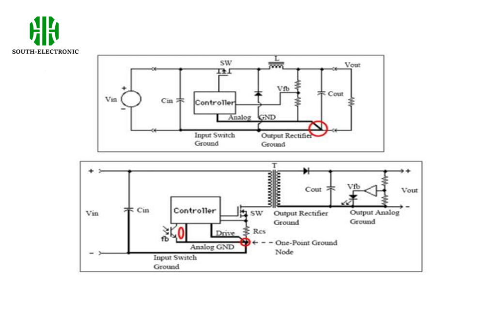
How to master power plane splitting for managing multiple voltages?
Mixed voltages fight for territory. Cross-talk corrupts signals when planes overlap improperly.
Split power planes isolate different voltages. Keep splits perpendicular to minimize noise coupling. Maintain clear moats between sections. Return currents need dedicated paths across boundaries to prevent antenna effects.
Voltage Zone Principles
| Isolation Strategy | Implementation | Purpose |
|---|---|---|
| Anti-etch gaps | 0.5mm minimum | Prevent arcing |
| Dedicated zones | Non-overlapping regions | Reduce crosstalk |
| Layer segregation | Adjacent layers for different voltages | Contain EMI |
Know your voltage domains first. Draw boundaries before routing. Never split sensitive analog planes. Place transition zones near board edges. Moats must be continuous. I once lost weeks debugging a power issue caused by a forgotten 0.3mm gap between zones. Use thermal reliefs for connections crossing splits. Signal traces should not straddle moats without return paths. Each voltage needs its kingdom.
What are the essentials for power plane integrity (decoupling, impedance, avoiding noise)?
Your IC sees noise as false signals. Power fluctuations create ghost commands and crashes.
Low impedance requires minimized loops. Place decoupling capacitors closest to IC power pins. Match capacitor values to noise frequencies. Separate analog/digital planes control interference. Layer stack design determines impedance.
Noise Fighting Tools
| Component | Placement Rule | Function |
|---|---|---|
| 0.1µF cap | <5mm from IC pin | Filters high-frequency noise |
| 10µF cap | Power inlet | Handles low-frequency ripple |
| Ferrite bead | Between noisy circuits | Blocks EMI propagation |
Start power analysis early. Calculate required capacitance per IC datasheet. Capacitors work at specific frequencies. Multiple sizes form defense lines. Vias add inductance which hurts transient response. Keep reference planes intact beneath components. Solid planes provide stable impedance. Avoid slots under critical traces. Proper grounding makes all other solutions work better.
Conclusion
Power planes form your PCB's circulatory system. Prioritize layer strategy, copper density, split management, and decoupling for robust designs every time.

