
Troubled by PCB failures? Confusing layer setups cause signal chaos, overheating, and costly redesigns. Master these critical layers to avoid disasters in your next project.
Essential PCB layers include signal layers for electrical connections, power/ground planes for voltage stability, substrate for structural support, solder mask for trace protection, and silkscreen for component labeling. Each layer ensures reliable performance and prevents system failures.

Now that we’ve mapped the core layers, let’s explore how they impact real-world performance. Understanding interactions between layers is key to building robust electronics.
How Do Different PCB Layers Affect the Board’s Performance and Reliability?
Ever wonder why some PCBs overheat while others fail prematurely? Layer designs directly control thermal limits and product lifespans. Poor layer planning causes real danger.
Signal layers minimize interference through careful routing. Ground planes reduce electromagnetic noise by 60%. Power planes stabilize voltage drops under load. Together, they prevent overheating, signal loss, and sudden system crashes.
Critical Layer Interactions
Layers collaborate like team players. Ignoring their relationships invites failure.
Thermal Management
Power planes spread heat away from chips. Thicker copper layers handle higher temperatures. I once saw a PCB melt because ground planes were too thin.
Signal Integrity
Noisy layers cause miscommunication. Proper spacing prevents crosstalk. High-speed signals need ground shielding below them.
| Layer Pair | Function | Reliability Boost |
|---|---|---|
| Signal + Ground | Reduces electromagnetic interference | 50% fewer errors |
| Power + Substrate | Dissipates heat | 30°C lower temps |
| Silkscreen + Solder | Prevents assembly mistakes | 20% faster QA |
Vibration Resistance
Flexible substrates absorb shocks. Denser layers handle industrial environments. Missing rigid layers lead to cracked traces.
What Are the Common Materials Used in PCB Layers?
Choosing wrong materials wastes thousands. Cheap substrates crack; inappropriate solder masks peel off. Material failure kills functionality without warning.
FR-4 epoxy laminate is the standard substrate. Copper foil creates signal/power layers. Liquid photo-imageable solder mask (LPI) protects copper. Silkscreen uses epoxy-based ink. Each material ensures thermal, electrical, and mechanical stability.
Material Selection Guide
Every layer demands specific properties. Mismatched materials cause field returns.
Substrate Materials
FR-4 dominates for cost and durability. High-frequency boards use polyimide or Rogers material. My industrial client switched to ceramic substrate for extreme heat.
Conductive Layers
Copper thickness (0.5oz-3oz) affects current handling. Gold plating prevents oxidation in humid areas. Some aerospace PCBs use aluminum cores.
| Material | Layer Usage | Key Strength | Weakness |
|---|---|---|---|
| Copper | Signal/Power Plane | High conductivity | Corrodes if exposed |
| FR-4 | Substrate | Cost-effective | Limited heat tolerance |
| LPI | Solder Mask | Precision coating | Requires UV curing |
| Epoxy ink | Silkscreen | Scratch-resistant | Slow drying time |
Coating Materials
Solder mask blocks solder bridging. ENIG (Gold) finishes protect contacts. Halogen-free materials meet environmental regulations.
How Does the PCB Stack-Up Process Work in Manufacturing?
Seem perfect on screen? Wrong stack-ups cause catastrophic failures. Layer order mistakes are invisible until testing. Getting sequence right saves months.
PCB stack-up arranges layers sequentially during fabrication. Engineers position signal layers between ground/power planes to reduce noise. Symmetric stacking prevents warping. Proper layer count matches complexity needs.
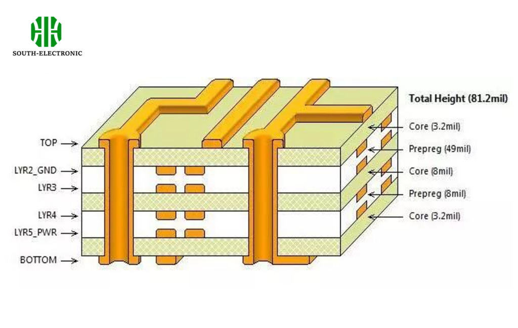
Step-by-Step Stacking
A 6-layer build taught me one mistake derails everything. Precision matters.
Planning Phase
Define layer count based on circuit complexity. High-speed designs need more ground planes. A drone controller required 10 layers for stability.
Sequencing Rules
Place ground layers adjacent to signals. Balance copper distribution. Asymmetric designs warp during reflow soldering.
| Layer # | Type | Critical Partner | Purpose |
|---|---|---|---|
| 1 | Top Signal | Layer 2 (Ground) | Component connections, routing |
| 2 | Ground | Layers 1 & 3 | Shields noise, provides reference |
| 3 | Inner Signal | Layer 2 & 4 | High-speed paths |
| 4 | Power | Layers 3 & 5 | Stable voltage delivery |
Verification Steps
Run simulations for heat, signal quality, and mechanical stress. Test prototypes via thermal cycling.
Conclusion
Layers form a PCB’s backbone. Materials and stack-up ensure reliability. Mastering these builds error-free electronics that perform under pressure.

