

Finding unexpected failures in your electronics? PCB damage halts operations and frustrates engineers. Identifying root causes saves time and money. This guide reveals critical failure triggers.
PCB failure typically stems from manufacturing flaws, environmental stress, soldering defects, and component degradation. Poor design choices, electrostatic discharge (ESD), and material aging also cripple circuit boards during operation. Proper inspection methods catch these early.
Let’s dissect each failure source systematically. Understanding these risks prepares you for effective troubleshooting pcb circuits. Practical repair strategies follow this breakdown.
How to Visually Inspect a PCB?
Seeing unusual board behavior? Visual checks catch 80% of PCB damage early. Grab a magnifier and bright light to start hunting flaws.
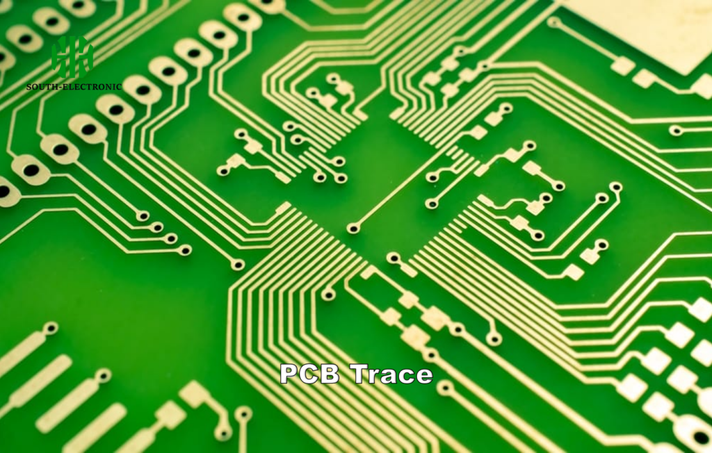
Thorough visual inspection examines soldering consistency, physical damage, and component alignment. Look for cracked traces, swollen capacitors, or discolored areas indicating heat stress. Document findings methodically before fix pcb board attempts.
Early detection prevents minor issues from escalating. I recall a thermostat PCB failure where burnt resistors were visible under magnification. Let’s systematize inspection steps:
Critical Visual Checkpoints
| Area | What to Check | Common Defects |
|---|---|---|
| Soldering | Joint shine and shape | Cold joints, bridging |
| Traces | Line continuity/width | Cracks, corrosion spots |
| Components | Orientation and discoloration | Burnt pcb marks, bent leads |
| Board Base | Warping or delamination | Blistering, bubbling layers |
Begin with clean magnification tools. Check solder joints under angled light—dull or grainy surfaces suggest cold joints. Trace inspections follow path continuity, especially near connectors receiving mechanical stress. Capacitor bulges or leaking electrolyte indicate failure. Finally, scan the board substrate for warping, which hints at thermal damage or moisture exposure. Such printed circuit board repair assessments take minutes but prevent hours of electrical debugging.
How to Fixing Broken Traces, Lifted Pads, and Poor Solder Joints?
Frustrated by intermittent connections? These physical defects disable devices but often yield to careful printed circuit board repair. Gather your micro-soldering gear.
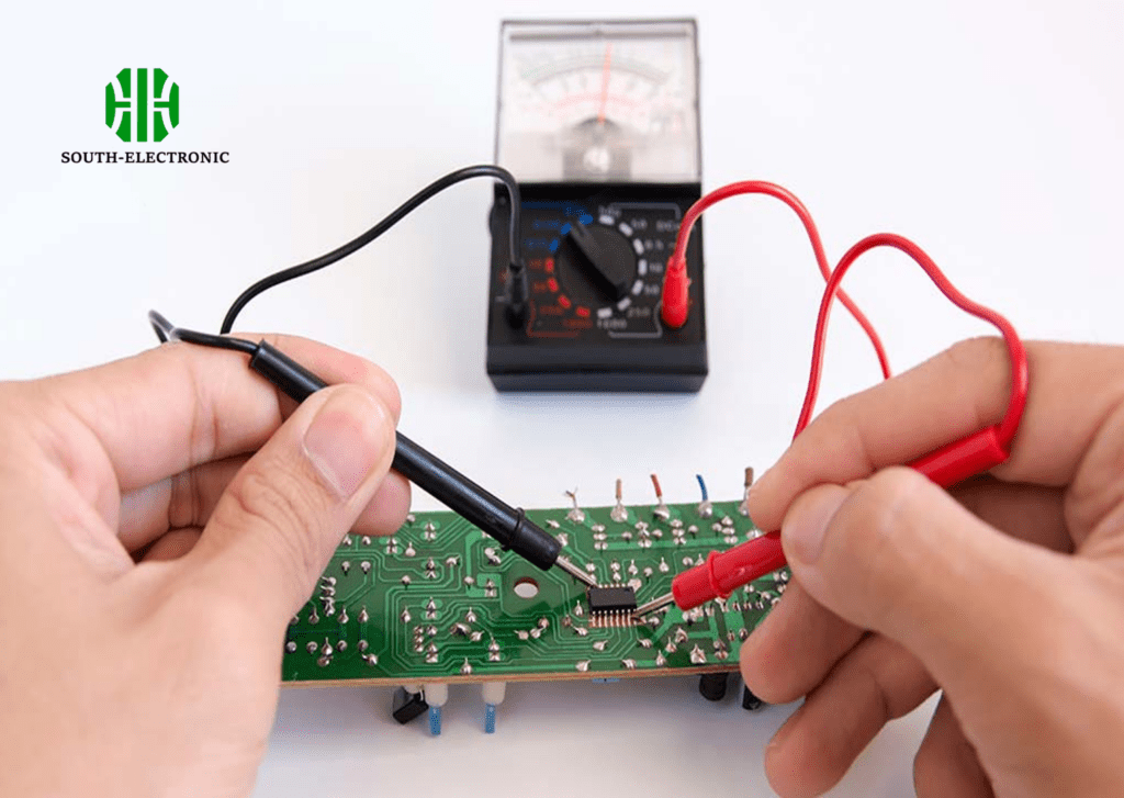
Repair involves scraping trace coatings, bridging breaks with wire, and re-adhering pads using epoxy. For solder joints, reheating with flux corrects cold connections. Always test continuity after fixes before reassembly.
During my early repair attempts, lifted pads taught me patience. Now I consider these systematic solutions:
Repair Techniques by Damage Type
| Failure | Tools Required | Repair Process |
|---|---|---|
| Broken Trace | X-Acto knife, enamel wire | Scrape insulation → Solder bridging wire |
| Lifted Pad | Epoxy, copper tape | Adhere replacement → Route new connection |
| Cold Joint | Flux, soldering iron | Reflow solder → Inspect fillet shape |
Start trace repairs by exposing copper beneath breaks using a precision blade. Bridge gaps with thin Kynar wire matching original trace thickness. For detached pads, secure alternatives with conductive epoxy or adhesive copper tape. Poor solder joints demand reheating at 300-350°C with added flux—watch for the telltale "flash" indicating proper flow. Always avoid excessive heat to prevent adjoining pads from lifting. Such fixes restore most boards unless carbonized damage exists.
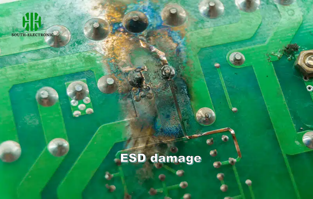
How to Assess and Fix Electrical Overstress Damage?
Smell ozone when devices fail? Electrical surges often leave invisible scars. Diagnostic rigor reveals shock-damaged components others miss.
Check surge pathways using thermal imaging and curve tracing. Replace blown fuses/varistors first. Test semiconductors for leakage. Isolate damaged sub-circuits before system-level testing to prevent cascading failures.

After a lightning strike fried a server PCB, I learned voltage spikes behave like termites. Surface clues deceive:
Electrical Overstress Indicators
| Evidence | Testing Approach | Recovery Potential |
|---|---|---|
| Charred Components | Visual/thermal inspection | Low – requires replacement |
| Hidden Trace Damage | Micro-ohmmeter scans | Moderate – if isolated |
| IC Latent Failure | Curve tracer analysis | Variable – test thoroughly |
Begin by identifying entry points like power ports or I/O connectors. Suspect clamping diodes and fuses near these zones. Use thermal cameras on powered boards; hot spots reveal shorted components. Semiconductor failures require removing and testing individual transistors—leakage current often outlives visible damage. For multi-layer board internal burns, consider sectional replacement. Document every step; burnt pcb areas may cause secondary issues weeks later.
Solutions for Common PCB Damage: Repair vs. Replacement & Preventing Failures
Hesitating between repair or new board? Cost-benefit analysis determines the right path. Prevention strategies also reduce future headaches significantly.
Minor damage affecting under 30% of components warrants repair. For multi-point failures or delaminated boards, replacement proves cheaper. Prevention includes conformal coating, surge protection, and thermal management during design.
Watching clients face this dilemma inspired this decision framework:
Damage Response Matrix
| Scenario | Recommended Action | Prevention Tactic |
|---|---|---|
| 1-2 Broken Traces | Repair | Reinforce high-stress zones |
| Burnt Components + Traces | Component-level repair | Improve heatsinking |
| Lifted Pads + Layer Separation | Replace board | Specify higher Tg materials |
| Recurring Failures | Redesign subsystem | Environmental sealing |
Prioritize repair when replacement boards cost 5x more than labor. For vintage gear, component-level fixes preserve functionality despite imperfections. Modern boards with HDI technology often require replacement due to micro-vias damage. Prevention starts with conformal coatings blocking moisture and dust. Always include tinned copper areas for grounding ESD straps during handling. Thermal simulations during design prevent hot spots causing premature aging. These steps convert reactive troubleshooting pcb circuits work into proactive reliability engineering.
Conclusion
Most PCB failures arise from preventable issues. Regular inspection, quick repairs for minor flaws, and smart design choices extend circuit life significantly. Invest in protection before damage occurs.

