

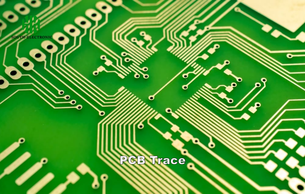
PCB wiring is the most labor-intensive and tedious process in the entire PCB design, which directly affects the performance of the PCB board. In this article, we will talk about some basic rules that need to be followed in the PCB wiring process.
Some rules that need to be followed in PCB wiring design
- Chamfering rules

Avoid sharp angles and right angles in PCB design, which will generate unnecessary radiation and poor process performance
- Device decoupling rules

Add necessary decoupling capacitors on the PCB to filter out interference signals on the power supply and stabilize the power supply signal. It is recommended that the power supply be connected to the power pin after passing through the filter capacitor.
- Ground loop rules

The minimum loop rule, that is, the loop area formed by the signal line and its loop should be as small as possible. The smaller the loop area, the less external radiation and the less interference received from the outside world.
- Shielding protection rules

Corresponding to the ground wire loop rule, it is actually to minimize the loop area of the signal as much as possible, which is more common in some important signals, such as clock signals and synchronization signals; for some particularly important and high-frequency signals, the copper axis cable shielding structure design should be considered, that is, the wires are isolated from top to bottom and left to right with ground wires, and how to effectively combine the shielding ground with the actual ground plane should also be considered.
- 3W rule

In order to reduce crosstalk between wires, the wire spacing should be large enough. When the center spacing of the wires is not less than 3 times the wire width, 70% of the electric fields can be kept from interfering with each other, which is called the 3W rule. If 98% of the electric fields do not interfere with each other, a spacing of 10W can be used
- 20H rule

Since the electric field between the power layer and the ground layer is changing, electromagnetic interference will be radiated outward at the edge of the board. It is called the edge effect. The solution is to shrink the power layer so that the electric field is only conducted within the range of the ground layer. Taking one H (the thickness of the dielectric between the power supply and the ground) as a unit, if the inward shrinkage is 20H, 70% of the electric field can be confined to the edge of the ground layer; if the inward shrinkage is 100H, 98% of the electric field can be confined.
What are the requirements for PCB wiring sequence?
In order to achieve the best wiring of PCB, the wiring sequence should be determined according to the sensitivity of various signal lines to crosstalk and the requirements of wire transmission delay. The signal lines that are preferentially routed should have their interconnection lines as short as possible. Generally, the wiring should be done in the following order:
-
Analog small signal lines;
-
Signal lines and small signal lines that are particularly sensitive to crosstalk;
-
System clock signal lines;
-
Signal lines that have high requirements for wire transmission delay:
-
General signal lines;
-
Static potential lines or other auxiliary lines.
How to Calculate PCB Trace Width?
Calculating the correct PCB trace width is vital to ensure your circuit works safely. Traces that are too narrow can overheat or fail under high current. I remember my first PCB project for a small robot. I used thin traces for the motor power lines, and they melted within minutes. That mistake taught me the importance of getting this right.
Here’s the basic process:
- Determine the maximum current: This depends on the components. For example, an LED might draw 20mA, but a motor could draw several amps. I use a multimeter to measure current in existing circuits or check component datasheets for new designs.
- Know the copper thickness: Most PCBs use 1 oz (35μm) or 2 oz (70μm) copper. Thicker copper handles more current. A 2 oz trace can carry about 1.5x more current than a 1 oz trace at the same width.
- Decide on temperature rise: A common goal is a 10°C or 20°C rise. Higher temperature rises are risky for sensitive components. For a car stereo amp I built, I aimed for 10°C to prevent overheating in a confined space.
There are two main ways to calculate trace width:
- Formulas: The IPC – 2152 standard has a formula that relates current, trace width, copper thickness, and temperature rise. For example, for 1 oz copper and 1A with 10°C rise, the formula might suggest ~10 mils (0.25mm). For 5A, it could be ~50 mils (1.27mm).
- Online calculators: Tools like those from ExpressPCB or ADC are easier. Just enter the current, copper thickness, and temperature rise. I always round up the result to the nearest standard width (e.g., 12 mils instead of 10 mils) for safety.
Don’t forget about voltage drop and trace length. Long traces (over 10cm) for low – voltage circuits (like 3.3V) can lose significant voltage due to resistance. In a WiFi sensor project, a 15cm trace for 5V caused a 0.5V drop until I widened it to 20 mils.
How to Read PCBs and Identify Components?
Reading a PCB starts with understanding its labels and components. I once spent hours repairing a broken router by identifying components one by one. Here’s how to do it:
- Use the Silkscreen Layer
The silkscreen (usually white print on the PCB) labels each component with a code:
- R1, R2…: Resistors
- C1, C2…: Capacitors
- U1, U2…: Integrated circuits (ICs)
- Q1, Q2…: Transistors
- D1, D2…: Diodes
On an old USB charger PCB, I saw "C5" near a cylindrical component with a "-" mark, so I knew it was an electrolytic capacitor.
- Identify Components by Appearance
- Resistors: Through – hole resistors have color bands. For example, brown – black – red – gold = 1kΩ ±5%. Surface – mount resistors have numerical codes like "104" = 100kΩ (10 x 10^4).
- Capacitors: Ceramic caps are small and rectangular (often with a "C" code). Electrolytic caps are larger, cylindrical, and have polarity marks.
- ICs: These have many pins and a part number (e.g., "ATmega328" is an Arduino microcontroller). I lookup part numbers on Digi – Key or Mouser to find datasheets.
- Transistors: Most have three leads. NPN transistors (like 2N2222) are common in amplifiers; PNP (like 2N3906) in switching circuits.
- Use Tools for Help
- Multimeter: Test resistance (for resistors), capacitance (for caps), or diode mode (to check diodes). I once used it to find a faulty resistor that looked fine but had drifted in value.
- Magnifying glass/USB microscope: These help read tiny labels on surface – mount components. I use a $20 USB microscope to see codes like "225" on a 0402 – size cap (2.2μF).
- Schematic (if available): Match PCB labels to the schematic. If there’s no schematic, trace connections with the multimeter’s continuity mode.
- Understand PCB Layout Patterns
- Power components: Voltage regulators (e.g., LM7805), large capacitors, and fuses are near the power input.
- Main ICs: Microcontrollers or processors are often in the center, with smaller components (resistors, caps) around them.
- Connectors: USB ports, headers, or switches are on the edges. On a Raspberry Pi HAT PCB, the GPIO header is clearly labeled on the edge.

Conclusion
Mastering these skills takes time, but each project builds your confidence. When calculating trace width, always prioritize safety over minimal width. When reading PCBs, start with simple boards and gradually move to complex ones.
I still remember the first time I successfully converted a PCB to a schematic for a broken lamp. Seeing the circuit on paper made the repair obvious: a faulty resistor had burned out. With these skills, you can troubleshoot, modify, and create electronics with confidence. Keep practicing, and don’t be afraid to ask for help or look up resources when stuck. Happy soldering!

