
This article will explain PCB-related terminology in detail. Let’s take a look.
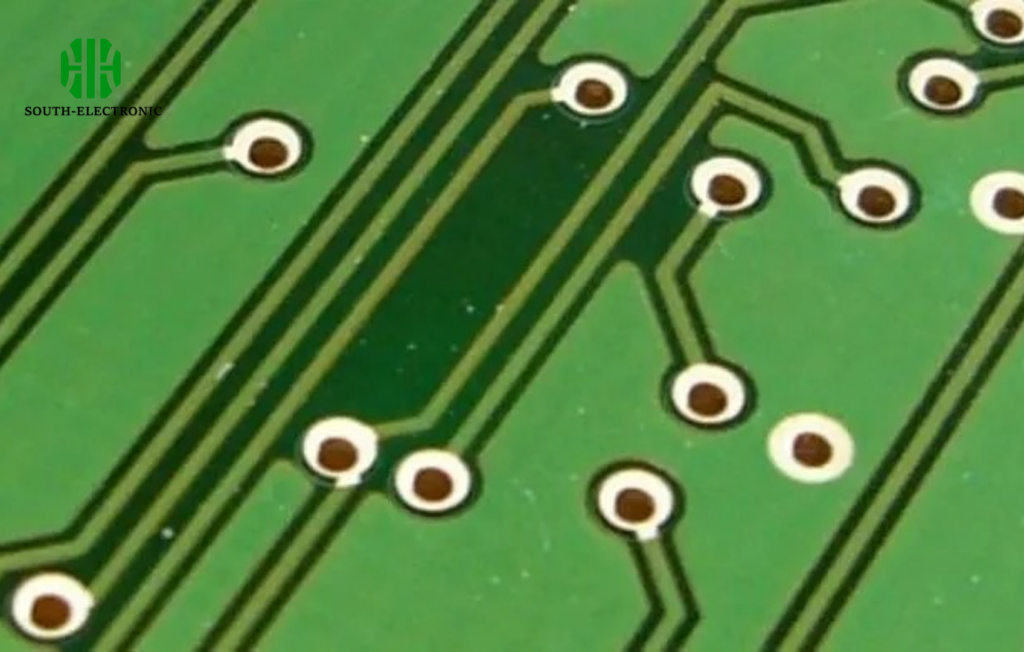
- Annular Ring:
The copper ring surrounding a plated-through hole on a PCB.

- DRC:
Design Rule Check, a process that checks a design for errors such as trace shorts, traces that are too thin, or holes that are too small.
- Drill Hit:
This term indicates the deviation between the specified drill hole location and the actual drill hole location. Incorrect drill centering caused by a dull drill bit is a common problem in PCB manufacturing.
The image above shows an example of an inaccurate drill hit.
-
Gold Finger:
An exposed metal pad on the edge of a board, typically used to connect two circuit boards, such as the edge of a computer expansion module, memory stick, or even an older game cartridge. -
Stamp Hole:
An alternative to V-cuts in board separation design. Using a series of holes creates a weak connection point, making it easier to separate a board from the panel.

- Pad:
A section of exposed metal on the PCB surface used for soldering components.
-
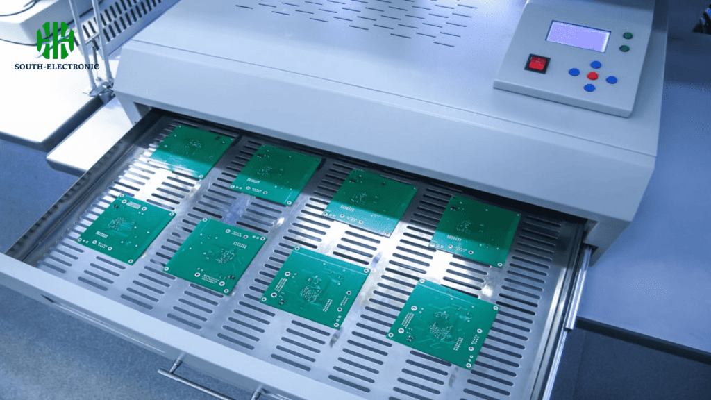
Panel:
A large circuit board made up of many smaller, separable boards. Automated PCB production equipment often experiences issues when producing smaller boards, so combining several boards together can speed up production. -
Stencil: A thin metal or plastic template placed on a PCB during assembly to allow solder to penetrate specific areas.
-
Pick-and-place:
A machine or process used to place components on a circuit board. -
Plane: A continuous section of copper on a circuit board, typically defined by edges rather than paths. Also called a copper fill.
-
Plated Via:
A hole in a PCB, consisting of a ring and plated wall. A plated via can be a connection point for a plug-in, a signal layer transition, or a mounting hole.
-
FABFM:
A plug-in resistor on a PCB. The two legs of the resistor have been inserted through a via in the PCB. The plated hole wall allows traces on both sides of the PCB to connect. -
Pogo pin:
A spring-loaded temporary contact point, typically used for testing or programming. -
Reflow:
The process of melting solder to connect the surface mount device (SMD) pad to the device pin.
- Slot:
Any non-circular hole on a PCB. Slots can be plated or unplated. Slots require additional cutting time, which can sometimes increase the cost of the board.
Note: Because the slotting tool is round, the edges of the slot cannot be perfectly square.
-
Solder paste:
A thick layer of solder paste is applied to the surface mount device pads through a stencil before placing the components on the PCB.
During the reflow process, the solder paste melts, creating a reliable electrical and mechanical connection between the pads and the device pins. Before placing components, briefly apply a layer of solder paste to the PCB. Remember to understand the definition of a stencil. -
Soldering pot:
A furnace used for soldering components. It typically contains a small amount of molten solder, which the board passes quickly through to solder exposed pins. -
Solder mask:
A protective film applied to copper to prevent short circuits, corrosion, and other problems.

-
Soldering:
Two connected pins on a component are mistakenly connected by a small drop of solder. -
Surface mount:
An assembly method in which components are simply placed on the board without inserting the pins through vias. -
Thermal pad:
A short trace connecting the pad to a plane. Without proper heat dissipation, it can be difficult to heat the pad to a sufficient temperature during soldering. Improper heat dissipation can result in a sticky pad and a relatively long reflow time.
On the left, the pad is connected to the ground plane via two short traces (thermal pads). On the right, the via is connected directly to the ground plane without a thermal pad.
- Trace:
A generally continuous copper path on a circuit board.
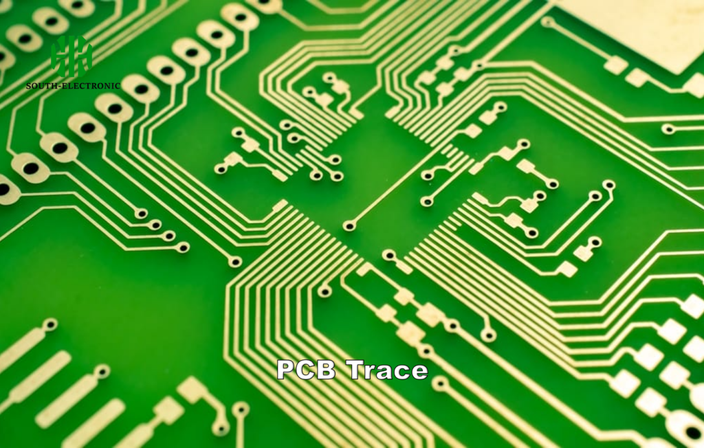
A thin trace connects the reset point to another location on the board, while a thicker trace connects to the 5V power point.
-
V-score:
A partial cut through the board that can be broken along this line. -
Via:
A hole in a board, typically used to switch a signal from one layer to another.
A plugged via is a via covered with solder mask to prevent soldering. Connector or device pin vias are typically not plugged because they require soldering.
Both sides of a plugged via on the same PCB. This via transfers the signal from the front side to the back side through a drilled hole in the board.
- Wave soldering:
A method of soldering plug-in components in which the board is passed through a molten solder furnace at a constant speed to produce a stable wave. The solder wave will solder the component pins and exposed pads together.

