
Struggling to visualize tiny electronics parts? Confused by assembly jargon? I remember my first PCB project – components looked like ant-sized specks! Let me demystify these terms that dominate modern gadget manufacturing.
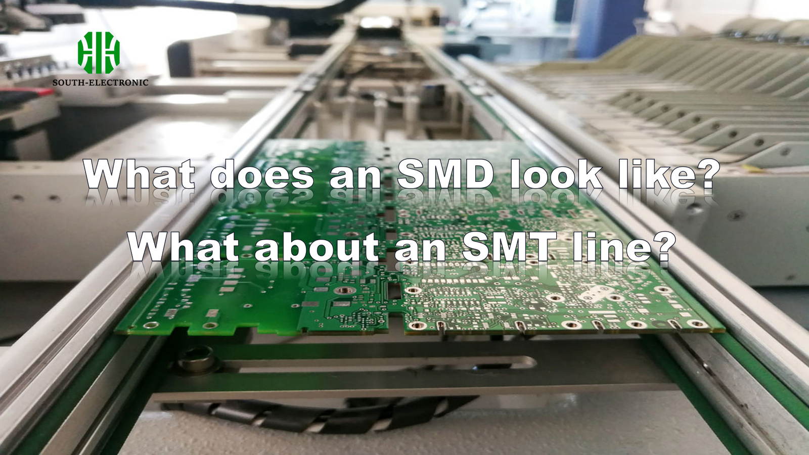
SMDs (Surface Mount Devices) are miniature flat chips with metallic pads instead of wires, while SMT lines are robotic factories that place and solder thousands of these per hour onto circuit boards, enabling mass production of compact phones, laptops and smart devices.
Seeing both pieces clarifies electronics design puzzles. Now, let’s peel back manufacturing layers through four critical angles shaping today’s tech world.
How does building with SMT differ from using SMDs alone?
Frustrated by slow hand-soldering? I once wasted hours aligning microscopic parts. SMDs alone are just raw materials – like bricks without masons.
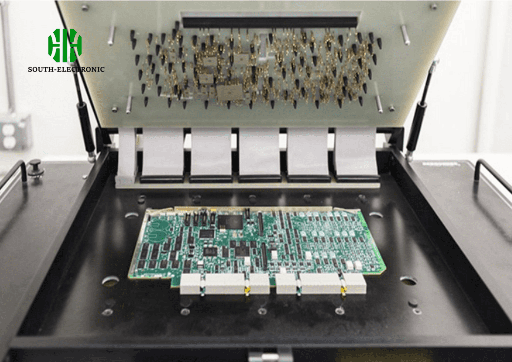
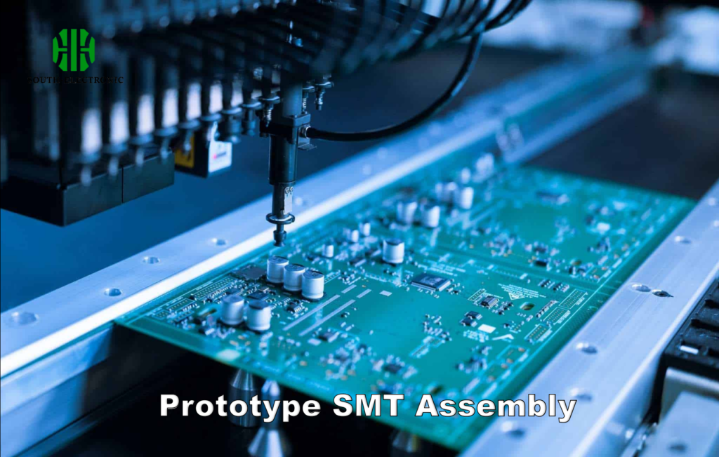
SMT transforms individual SMDs into functional systems using automated assembly lines featuring precision robots, ovens, and QC scanners, while manually handling SMDs limits scale and reliability for commercial production.
Let’s unpack the core process differences:
Component vs. System Implementation
SMDs represent singular elements ready for installation, whereas SMT deploys integrated manufacturing ecosystems. Think scissors versus automated textile plants.
Workflow Complexity
Manual SMD placement demands painstaking human effort – tweezers, magnifiers, steady hands. An SMT line handles soldering, inspection, and placement seamlessly through these stages:
| Step | Manual SMD Work | SMT Automated Line |
|---|---|---|
| Placement | Human with tweezers | High-speed robots |
| Soldering | Handheld iron | Reflow oven conveyor |
| Inspection | Eye/microscope | Automated AOI cameras |
| Daily Output | 10-50 boards | 10,000+ boards |
SMT’s automation cuts errors from 30% to near zero – crucial for iPhone-grade consistency. Without the line, we couldn’t scale beyond hobbyist prototypes due to fatigue and tolerances under 0.01mm.
Why did one of SMT or THT become the champion of modern electronics?
Annoyed by bulky old radios? Through-Hole Technology (THT) dominated last century, but I’ve witnessed its decline as gadgets shrank. THT’s wire-through-hole design consumed excessive space.
SMT superseded THT by enabling smaller, faster, cheaper electronics – utilizing both sides of PCBs without drilling holes, allowing smartphone slimness impossible with vintage through-hole components.

Three innovations fueled this victory:
Miniaturization Revolution
SMT’s elimination of leads and holes saved 70-90% space versus THT. Tablets would be notebook-thick using old tech.
Manufacturing Speed
THT required sequential manual insertion. SMT robots place 100+ components in seconds – critical for meeting global gadget demand.
Cost Efficiency
No drilling and lower material use dropped production costs by 60% since the 2000s. This democratized advanced electronics worldwide.
Do I always use SMDs with SMT?
Think SMT mandates SMDs? Early in my career, I wrongly assumed exclusivity. Hybrid boards prove otherwise – blending both strategies creatively.
SMT primarily handles SMDs but adapts for odd-shaped non-SMD parts using specialized nozzles, though 95% of modern assemblies prioritize SMD compatibility to maximize automation benefits and miniaturization.

Real-world flexibility explained:
When Exceptions Occur
Transformers, large capacitors, or connectors sometimes require through-hole mounting due to weight or heat constraints. SMT lines handle these using modified stations.
Why Pure SMD Dominates
The industry trend favors full SMD solutions to eliminate secondary soldering processes. This table shows why exceptions are dwindling:
| Factor | SMD Advantage | Non-SMD Limitation |
|---|---|---|
| Automation | Fully programmable | Manual intervention |
| Board space | Uses both sides | Single-side mounting |
| Throughput | 3x faster assembly | Bottlenecks |
| Rework | Hot air reversible | Complex desoldering |
With advanced packaging like QFNs and BGAs, even 99% of designs now avoid through-holes.
Why is fixing tiny phones with SMD vs THT components so much harder?
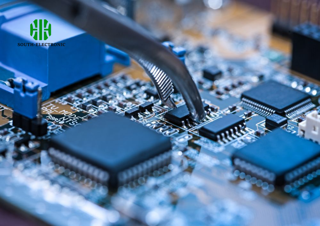
Ever tried phone repair? I once destroyed three microchips with one shaky hand. THT gave visible pins; SMDs hide connections under microscopic bodies.
Micro-soldering SMDs demands 10x magnification, sub-millimeter precision tools, and micro-solder balls, whereas THT components offer accessible leg contacts for traditional irons – making modern rework a specialist’s high-stress puzzle.
Let’s break down repair nightmares:
Tool & Skill Gaps
Dime-sized circuit boards require $2,000 microscopes and 0.2mm tips. Slip by 0.5mm fries neighboring chips – THT tolerated 2mm errors.
Structural Challenges
SMDs often lack visible solder joints. Common phone repairs like charging ports illustrate this:
| Issue | SMD Challenge | THT Parallel |
|---|---|---|
| Connections | Joints hidden beneath chip | Visible solder joints |
| Removal | Hot air gun risks warping nearby parts | Direct pin heating |
| Alignment | Placement precision ±0.1mm needed | ±1mm acceptable |
| Heat Sensitivity | Multilayer boards delaminate easily | Single-layer resilience |
Voids under chips are invisible without X-ray machines – explaining why repair shops charge premium rates.
Conclusion
SMDs enable tiny gadgets, while SMT lines build them at scale. Together, they’ve revolutionized electronics manufacturing, but created complex repair realities requiring specialized solutions.

